
Datasheet


15
LTC2846
sn2846 2846fs
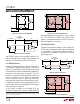
Figure 28. Charge Pump
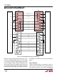
Figure 27. V.35 Receiver Configuration
Figure 26. Typical V.35 Interface
APPLICATIO S I FOR ATIO
WUUU
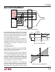
In V.28 mode, S3 is closed inside the LTC2846/LTC2844
which connects a 6k (R8) impedance to ground in parallel
with 20k (R5) plus 10k (R6) for a combined impedance of
5k as shown in Figure 25. Proper termination is only pro-
vided when the B input of the receivers is floating, since S1
of the LTC2846’s R2 and R3 receivers remains on in V.28
mode
1
. The noninverting input is disconnected inside the
LTC2846/LTC2844 receiver and connected to a TTL level
reference voltage to give a 1.4V receiver trip point.
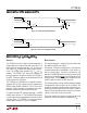
V.35 Interface
A typical V.35 balanced interface is shown in Figure 26. A
V.35 differential generator with outputs A and B and
ground C is connected to a differential receiver with input
A' connected to A, input B' connected to B, and ground C'
connected via the signal return to ground C. The V.35
interface requires a T or delta network termination at the
receiver end and the generator end. The receiver differen-
tial impedance measured at the connector must be
A
A
'
B
C
B
'
C
'
GENERATOR
BALANCED
INTERCONNECTING
CABLE
LOAD
CABLE
TERMINATION
RECEIVER
2846 F26
50Ω
125Ω
50Ω
50Ω
125Ω
50Ω
R3
124Ω
R5
20k
LTC2846
RECEIVER
2846 F27
A
'
B
'
C
'
R1
51.5Ω
R8
6k
S2
S3
R2
51.5Ω
R6
10k
R7
10k
GND
R4
20k
S1
100Ω␣ ±10Ω, and the impedance between shorted termi-
nals (A' and B') and ground (C') must be 150Ω ±15Ω.
In V.35 mode, both switches S1 and S2 inside the LTC2846
are on, connecting a T network impedance as shown in
Figure 27. The 30k input impedance of the receiver is
placed in parallel with the T network termination, but does
not affect the overall input impedance significantly.
The generator differential impedance must be 50Ω to
150Ω and the impedance between shorted terminals (A
and B) and ground (C) must be 150Ω ±15Ω.
No-Cable Mode
The no-cable mode (M0 = M1 = M2 = 1) is intended for
the case when the cable is disconnected from the con-
nector. The charge pump, bias circuitry, drivers and
receivers are turned off, the driver outputs are forced into
a high impedance state, and the
V
CC
supply current to the
transceiver drops to less than 300µA while its
V
IN
supply
current drops to less than 10µA. Note that the LTC2846’s
R2 and R3 receivers continue to be terminated by a 103
Ω
differential impedance.
Charge Pump
The LTC2846 uses an internal capacitive charge pump to
generate V
DD
and V
EE
as shown in Figure 28. A voltage
doubler generates about 8V on V
DD
and a voltage inverter
generates about – 7.5V on V
EE
. Three 1µF surface mounted
tantalum or ceramic capacitors are required for C1, C2 and
C3. The V
EE
capacitor C4 should be a minimum of 3.3µF.
All capacitors are 16V and should be placed as close as
possible to the LTC2846 to reduce EMI.
33
32
31
30
2846 F28
7
6
5
8
C3
1µF
C5
10µF
5V
C1
1µF
C2
1µF
C4
3.3µF
LTC2846
V
DD
C1
+
C1
–
V
CC
C2
+
C2
–
V
EE
GND
+