
Datasheet


17
LTC2846
sn2846 2846fs
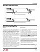
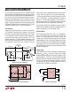
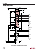
A port with one DB-25 connector, that can be configured
for either DTE or DCE operation is shown in Figure 33. The
configuration requires separate cables for proper signal
routing in DTE or DCE operation. For example, in DTE
mode, the TXD signal is routed to Pins 2 and 14 via the
LTC2846’s Driver 1. In DCE mode, Driver 1 now routes the
RXD signal to Pins 2 and 14.
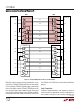
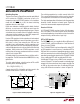
Multiprotocol Interface with RL, LL, TM
and a DB-25 Connector
If the RL, LL and TM signals are implemented, there are not
enough drivers and receivers available in the LTC2846/
LTC2844. In Figure 34, the required control signals are
handled by the LTC2845. The LTC2845 has an additional
single-ended driver/receiver pair that can handle two more
optional control signals such as TM and RL.
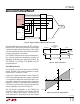
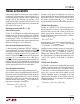
Cable-Selectable Multiprotocol Interface
A cable-selectable multiprotocol DTE/DCE interface is
shown in Figure 35. The select lines M0, M1 and DCE/DTE
are brought out to the connector. The mode is selected by
the cable by wiring M0 (connector Pin 18) and M1 (con-
nector Pin 21) and DCE/DTE (connector Pin 25) to ground
(connector Pin 7) or letting them float. If M0, M1 or
DCE/DTE is floating, internal pull-up current sources will
pull the signals to V
IN
. The select bit M2 is floating, and
therefore, internally pulled high. When the cable is pulled
out, the interface will go into the no-cable mode.
Power Dissipation Calculations
The LTC2846 takes in a 3.3V supply and produces a 5V V
CC
with an internal switcher at approximately 80% efficiency.
V
DD
and V
EE
are in turn produced from V
CC
with an internal
charge pump at approximately 80% and 70% efficiency
respectively. Current drawn internally from V
DD
or V
EE
translates directly into a higher I
CC
. The LTC2846 dissi-
pates power according to the equation:
P
DISS(2846)
= 125% • (V
CC
• I
CC
)
– N
D
• P
RT
+ N
R
• P
RT
(1)
TYPICAL APPLICATIO S
U
P
RT
refers to the power dissipated by each driver in a
receiver termination on the far end of the cable while N
D
is
the number of drivers. Conversely, current from the far
end drivers dissipate power N
R
• P
RT
in the internal
receiver termination where N
R
is the number of receivers.
LTC2846 Power Dissipation
Consider an LTC2846 in X.21, DCE mode (three V.11
drivers and two V.11 receivers). From the Electrical Char-
acteristics Table, I
CC
at no load = 14mA, I
CC
at full load =
100mA. Each receiver termination is 100Ω (R
RT
) and
current going into each receiver termination = (100mA –
14mA)/3 = 28.7mA (I
RT
).
P
RT
= (I
RT
)
2
• R
RT
(2)
From Equation (2), P
RT
= 82.4mW and from Equation (1),
DC power dissipation P
DISS(2846)
= 125% • (5V • 100mA)
– 3 • 82.4mW + 2 • 82.4mW = 543mW.
Consider the above example running at a baud rate of
10MBd. From the Typical Characteristic for “V.11 Mode
I
CC
vs Data Rate,” the I
CC
at 10MBd is 160mA. I
CC
increases with baud rate due to driver transient dissipa-
tion. From Equation (1), AC power dissipation P
DISS(2846)
= 125% • (5V • 160mA) –3 • 82.4mW + 2 • 82.4mW =
918mW.
LTC2845 Power Dissipation
If a LTC2845 is used to form a complete DCE port with the
LTC2846, it will be running in the X.21 mode (three V.11
drivers and two V.10 drivers, two V.11 receivers and two
V.10 receivers, all with internal 30k termination). In addi-
tion to V
CC
, it uses the V
DD
and V
EE
outputs from the
LTC2846. Negligible power is dissipated in the large
internal receiver termination of the LTC2845 so the N
R
•
P
RT
term of Equation (1) can be omitted. Thus Equation (1)
is modified as follows:
P
DISS(2845)
= (V
CC
• I
CC
) + (V
DD
• I
DD
)