
Datasheet


7
LTC2846
sn2846 2846fs
UU
U
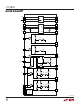
PI FU CTIO S
NC (Pin 1): No Connect.
PGND (Pin 2): Boost Switching Regulator Power Ground.
Tie PGND to SGND.
V
IN
(Pin 3): Input Supply Pin. Input supply to boost
switching regulator. 3V ≤ V
IN
≤ 3.6V. Bypass with a 10µF
capacitor to ground.
SHDN (Pin 4): Boost Switching Regulator Shutdown Pin.
Tie to 2.4V or more to enable regulator. Ground to shut
down.
C1
–
␣ (Pin 5): Capacitor C1 Negative Terminal. Connect a
1µF capacitor between C1
+
and C1
–
.
C1
+
(Pin 6): Capacitor C1 Positive Terminal. Connect a
1µF capacitor between C1
+
and C1
–
.
V
DD
(Pin 7): Generated Positive Supply Voltage for
V.28. Connect a 1µF capacitor to ground.
V
CC
(Pin 8): Input Supply Pin. Input supply to trans-
ceiver. 4.75V ≤ V
CC
≤ 5.25V. Connect to output of switch-
ing regulator.
D1 (Pin 9): TTL Level Driver 1 Input.
D2 (Pin 10): TTL Level Driver 2 Input.
D3 (Pin 11): TTL Level Driver 3 Input.
R1 (Pin 12): CMOS Level Receiver 1 Output with Pull-Up
to V
IN
when Three-Stated.
R2 (Pin 13): CMOS Level Receiver 2 Output with Pull-Up
to V
IN
when Three-Stated.
R3 (Pin 14): CMOS Level Receiver 3 Output with Pull-Up
to V
IN
when Three-Stated.
M0 (Pin 15): TTL Level Mode Select Input 0 with Pull-Up
to V
IN
. See Table 1.
M1 (Pin 16): TTL Level Mode Select Input 1 with Pull-Up
to V
IN
. See Table 1.
V
IN
(Pin 17): Input Supply Pin. Input supply to transceiver.
3V ≤ V
IN
≤ 3.6V. Connect to Pin 3.
M2 (Pin 18): TTL Level Mode Select Input 2 with Pull-Up
to V
IN
. See Table 1.
DCE/DTE (Pin 19): TTL Level Mode Select Input with
Pull-Up to V
IN
. See Table 1.
R3 B (Pin 20): Receiver 3 Noninverting Input.
R3 A (Pin 21): Receiver 3 Inverting Input.
R2 B (Pin 22): Receiver 2 Noninverting Input.
R2 A (Pin 23): Receiver 2 Inverting Input.
D3/R1 B (Pin 24): Receiver 1 Noninverting Input and
Driver 3 Noninverting Output.
D3/R1 A (Pin 25): Receiver 1 Inverting Input and Driver 3
Inverting Output.
D2 B (Pin 26): Driver 2 Noninverting Output.
D2 A (Pin 27): Driver 2 Inverting Output.
D1 B (Pin 28): Driver 1 Noninverting Output.
D1 A (Pin 29): Driver 1 Inverting Output.
GND (Pin 30): Transceiver Ground.
V
EE
(Pin 31): Generated Negative Supply Voltage. Connect
a 3.3µF capacitor to GND.
C2
–
(Pin 32): Capacitor C2 Negative Terminal. Connect a
1µF capacitor between C2
+
and C2
–
.
C2
+
(Pin 33): Capacitor C2 Positive Terminal. Connect a
1µF capacitor between C2
+
and C2
–
.
SGND (Pin 34): Boost Switching Regulator Signal Ground.
Tie PGND to SGND.
FB (Pin 35): Boost Switching Regulator Feedback Pin.
Reference voltage is 1.255V. Connect resistive divider tap
here. Minimize trace area at FB.
SW (Pin 36): Boost Switching Regulator Switch Pin.
Connect inductor/diode here. Minimize trace area at this
pin to reduce EMI.