
Datasheet

10
LTC2847
sn2847 2847fs
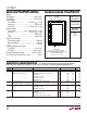
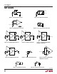
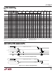
Figure 15. V.28 Driver Propagation Delays
Figure 16. V.28 Receiver Propagation Delays
SWITCHI G TI E WAVEFOR S
UWW
APPLICATIO S I FOR ATIO
WUUU
3V
0V
1.5V
0V
–3V
3V
1.5V
0V
3V
–3V
t
PHL
t
f
V
O
–V
O
D
A
t
PLH
t
r
2847 F15
SR =
6V
t
f
SR =
6V
t
r
V
IH
V
IL
1.5V
1.65V
1.5V
1.65V
t
PHL
V
OH
V
OL
A
R
t
PLH
2847 F16
Overview
The LTC2847 consists of a charge pump and a 3-driver/
3-receiver transceiver. The 5V V
CC
input powers the charge
pump and transceiver. The charge pump generates the
V
DD
and V
EE
supplies. The LTC2847’s
V
DD
and V
EE
supplies can be used to power a companion chip like the
LTC2845. The V
IN
input powers the digital interface in-
cluding the receiver output drivers. Having a separate pin
to power the digital interface allows the flexibility of
controlling the receiver output swing to interface with 5V
or 3.3V logic.
The LTC2847 and LTC2845 form a complete software-
selectable DTE or DCE interface port that supports the
RS232, RS449, EIA530, EIA530-A, V.35, V.36 and X.21
protocols. Cable termination is provided on-chip, elimi-
nating the need for discrete termination designs.
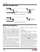
A complete DCE-to-DTE interface operating in EIA530
mode is shown in Figure 17. The LTC2847 half of each port
is used to generate and appropriately terminate the
clock and data signals. The LTC2845 is used to generate
the control signals along with LL (local loopback),
RL (Remote Loop-Back), TM (Test Mode) and RI (Ring
Indicate).
Mode Selection
The interface protocol is selected using the mode select
pins M0, M1 and M2 (see Table 1).
For example, if the port is configured as a V.35 interface,
the mode selection pins should be M2 = 1, M1 = 0, M0 =␣ 0.
For the control signals, the drivers and receivers will
operate in V.28 (RS232) electrical mode. For the clock and
data signals, the drivers and receivers will operate in V.35
electrical mode. The DCE/DTE pin will configure the port
for DCE mode when high, and DTE when low.
The interface protocol may be selected simply by plugging
the appropriate interface cable into the connector. The
mode pins are routed to the connector and are left uncon-
nected (1) or wired to ground (0) in the cable as shown in
Figure 18. The internal pull-up current sources will ensure
a binary 1 when a pin is left unconnected.
The mode selection may also be accomplished by using
jumpers to connect the mode pins to ground or V
IN
.