
Datasheet

12
LTC2847
sn2847 2847fs
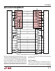
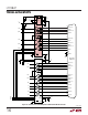
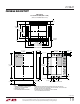
Figure 18. Single Port DCE V.35 Mode Selection in the Cable
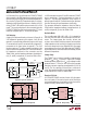
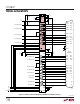
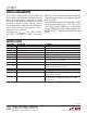
Figure 20. V.10 Receiver Input Impedance
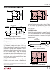
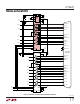
Figure 19. Typical V.10 Interface
APPLICATIO S I FOR ATIO
WUUU
selected. Switching the terminations with FETs is difficult
because the FETs must remain off when the signal voltage
is beyond the supply voltage. Alternatively, custom cables
may contain termination in the cable head or route signals
to various terminations on the board.
The LTC2847/LTC2845 chip set solves the cable termina-
tion switching problem by automatically providing the
appropriate termination and switching on-chip for the
V.10 (RS423), V.11 (RS422), V.28 (RS232) and V.35
electrical protocols.
V.10 (RS423) Interface
All V.10 drivers and receivers necessary for the RS449,
EIA530, EIA530-A, V.36 and X.21 protocols are imple-
mented on the LTC2845.
A typical V.10 unbalanced interface is shown in Figure 19.
A V.10 single-ended generator with output A and ground
C is connected to a differential receiver with input A' con-
nected to A, and ground C' connected via the signal return
to ground C. Usually, no cable termination is required for
V.10 interfaces, but the receiver inputs must be compliant
with the impedance curve shown in Figure 20.
The V.10 receiver configuration in the LTC2845 is shown
in Figure 21. In V.10 mode, switch S3 inside the LTC2845
is turned off. The noninverting input is disconnected
inside the LTC2845 receivers and connected to ground.
NC
NC
CABLE
2847 F18
LTC2847
LTC2845
CONNECTOR
(DATA)
M0
M1
M2
DCE/DTE
DCE/DTE
M2
M1
M0
(DATA)
AA
'
CC
'
GENERATOR
BALANCED
INTERCONNECTING
CABLE
LOAD
CABLE
TERMINATION
RECEIVER
2847 F19
I
Z
V
Z
–10V
–3.25mA
3.25mA
–3V
3V 10V
2847 F20