
Datasheet

LTC2850/LTC2851/LTC2852
12
285012fd
applicaTions inForMaTion
High Speed Considerations
A ground plane layout is recommended. A 0.1µF bypass
capacitor less than one-quarter inch away from the V
CC
pin
is also recommended. The PC board traces connected to
signals A/B and Z/Y should be symmetrical and as short
as possible to maintain good differential signal integrity.
To minimize capacitive effects, the differential signals
should be separated by more than the width of a trace
and should not be routed on top of each other if they are
on different signal planes.
Care should be taken to route outputs away from any
sensitive inputs to reduce feedback effects that might
cause noise, jitter, or even oscillations. For example, in
the full-duplex devices, DI and A/B should not be routed
near the driver or receiver outputs.
The logic inputs have 150mV of hysteresis to provide noise
immunity. Fast edges on the outputs can cause glitches in
the ground and power supplies which are exacerbated by
capacitive loading. If a logic input is held near its threshold
(typically 1.5V), a noise glitch from a driver transition may
exceed the hysteresis levels on the logic and data input
285012 F14
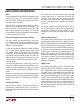
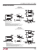
DATA RATE (bps)
CABLE LENGTH (FT)
10k 1M 10M100k 100M
100
1k
10
10k
RS485/RS422
MAX DATA RATE
LTC2850/
LTC2851/LTC2852
MAX DATA RATE
Figure 14. Cable Length vs Data Rate
(RS485/RS422 Standard Shown in Solid Line)
pins causing an unintended state change. This can be
avoided by maintaining normal logic levels on the pins
and by slewing inputs through their thresholds by faster
than 1V/µs when transitioning. Good supply decoupling
and proper driver termination also reduce glitches caused
by driver transitions.
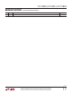
Cable Length vs Data Rate
For a given data rate, the maximum transmission distance
is bounded by the cable properties. A curve of cable length
vs data rate compliant with the RS485/RS422 standards
is shown in Figure 14. Three regions of this curve reflect
different performance limiting factors in data transmis-
sion. In the flat region of the curve, maximum distance
is determined by resistive losses in the cable. The down-
ward sloping region represents limits in distance and
data rate due to AC losses in the cable. The solid vertical
line represents the specified maximum data rate in the
RS485/RS422 standards. The dashed lines at 20Mbps
show the maximum data rates of the LTC2850, LTC2851
and LTC2852.
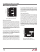
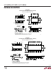
Figure 13. Supply Current vs Data Rate
DATA RATE (Mbps)
0.1
20
SUPPLY CURRENT (mA)
60
70
80
1 10 100
285012 F13
50
40
30
R
DIFF
= 54Ω
C
L
= 1000pF
C
L
= 100pF