
Datasheet

LTC2850/LTC2851/LTC2852
5
285012fd
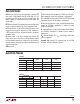
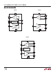
swiTching characTerisTics
Note 1: Stresses beyond those listed under Absolute Maximum Ratings
may cause permanent damage to the device. Exposure to any Absolute
Maximum Rating condition for extended periods may affect device
reliability and lifetime. High temperatures degrade operating lifetimes.
Operating lifetime is derated at temperatures greater than 105°C.
Note 2: All currents into device pins are positive; all currents out of device
pins are negative. All voltages are referenced to device ground unless
otherwise specified.
The l denotes the specifications which apply over the full operating
temperature range, otherwise specifications are at T
A
= 25°C. V
CC
= 3.3V, unless otherwise noted. (Note 2)
SYMBOL PARAMETER CONDITIONS MIN TYP MAX UNITS
Driver
f
MAX
Maximum Data Rate (Note 3)
l
20 Mbps
t
PLHD
, t
PHLD
Driver Input to Output
R
DIFF
= 54Ω, C
L
= 100pF (Figure 4)
l
10 50 ns
Δt
PD
Driver Input to Output Difference
|t
PLHD
– t
PHLD
|
R
DIFF
= 54Ω, C
L
= 100pF (Figure 4)
l
1 6 ns
t
SKEWD
Driver Output Y to Output Z
R
DIFF
= 54Ω, C
L
= 100pF (Figure 4)
l
1 ±6 ns
t
RD
, t
FD
Driver Rise or Fall Time
R
DIFF
= 54Ω, C
L
= 100pF (Figure 4)
l
4 12.5 ns
t
ZLD
, t
ZHD
,
t
LZD
, t
HZD
Driver Enable or Disable Time
R
L
= 500Ω, C
L
= 50pF, RE = 0V (Figure 5)
(LTC2850, LTC2852)
l
70 ns
t
ZHSD
, t
ZLSD
Driver Enable from Shutdown
R
L
= 500Ω, C
L
= 50pF, RE = V
CC
(Figure 5)
(LTC2850, LTC2852)
l
8 µs
t
SHDN
Time to Shutdown
R
L
= 500Ω, C
L
= 50pF, (DE = ↓, RE = V
CC
)
or (DE = 0V, RE = ↑) (Figure 5) (LTC2850,
LTC2852)
l
100 ns
Receiver
t
PLHR
, t
PHLR
Receiver Input to Output C
L
= 15pF, V
CM
= 1.5V, |V
AB
| = 1.5V,
t
R
and t
F
< 4ns (Figure 6)
l
50 70 ns
t
SKEWR
Differential Receiver Skew
|t
PLHR
– t
PHLR
|
C
L
= 15pF (Figure 6)
l
1 6 ns
t
RR
, t
FR
Receiver Output Rise or Fall Time C
L
= 15pF (Figure 6)
l
3 12.5 ns
t
ZLR
, t
ZHR
,
t
LZR
, t
HZR
Receiver Enable/Disable R
L
=1k, C
L
=15pF, DE = V
CC
(Figure 7)
(LTC2850, LTC2852)
l
50 ns
t
ZHSR
, t
ZLSR
Receiver Enable from Shutdown R
L
= 1k, C
L
= 15pF, DE = 0V (Figure 7)
(LTC2850, LTC2852)
l
8 µs
Note 3: Maximum data rate is guaranteed by other measured parameters
and is not tested directly.
Note 4: This IC includes overtemperature protection that is intended
to protect the device during momentary overload conditions.
Overtemperature protection activates at a junction temperature exceeding
150°C. Continuous operation above the specified maximum operating
junction temperature may result in device degradation or failure.
elecTrical characTerisTics
The l denotes the specifications which apply over the full operating
temperature range, otherwise specifications are at T
A
= 25°C. V
CC
= 3.3V, unless otherwise noted. (Note 2)
SYMBOL PARAMETER CONDITIONS MIN TYP MAX UNITS
Supplies
I
CCS
Supply Current in Shutdown Mode DE = 0V, RE = V
CC
,
LTC2850, LTC2852 (C and I-Grade)
LTC2850, LTC2852 (H-Grade)
l
l
0
0
5
15
µA
µA
I
CCR
Supply Current in Receive Mode DE = 0V, RE = 0V (LTC2850, LTC2852)
l
370 900 µA
I
CCT
Supply Current in Transmit Mode No Load, DE = V
CC
, RE = V
CC
(LTC2850,
LTC2852)
l
450 1000 µA
I
CCTR
Supply Current with Both Driver and
Receiver Enabled
No Load, DE = V
CC
, RE = 0V
l
450 1000 µA