
Datasheet

LTC2850/LTC2851/LTC2852
9
285012fd
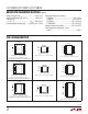
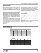
FuncTion Tables
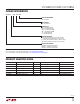
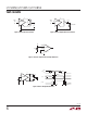
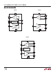
pin FuncTions
RO: Receiver Output. If the receiver output is enabled (RE
low) and A > B by 200mV, then RO will be high. If A < B
by 200mV, then RO will be low. If the receiver inputs are
open, shorted, or terminated without a valid signal, RO
will be high.
RE: Receiver Enable. A low enables the receiver. A high input
forces the receiver output into a high impedance state.
DE: Driver Enable. A high on DE enables the driver. A low
input will force the driver outputs into a high impedance.
If RE is high with DE low, the part will enter a low power
shutdown state.
DI: Driver Input. If the driver outputs are enabled (DE
high), then a low on DI forces the driver positive output
low and negative output high. A high on DI, with the driver
outputs enabled, forces the driver positive output high and
negative output low.
GND: Ground.
Y: Noninverting Driver Output for LTC2851 and LTC2852.
High impedance when driver disabled or unpowered.
Z: Inverting Driver Output for LTC2851 and LTC2852. High
impedance when driver disabled or unpowered.
A: Noninverting Receiver Input (and Noninverting Driver
Output for LTC2850). Impedance is >96kΩ in receive
mode or unpowered.
B: Inverting Receiver Input (and Inverting Driver Output
for LTC2850). Impedance is >96kΩ in receive mode or
unpowered.
V
CC
: Positive Supply. 3V < V
CC
< 3.6V. Bypass with 0.1µF
ceramic capacitor.
Exposed Pad: Ground. The exposed pads on the DFN
packages must be soldered to ground.
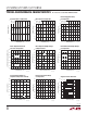
LTC2850
Logic Inputs
Mode A, B RO
DE RE
0 0 Receive R
IN
Driven
0 1 Shutdown R
IN
Hi-Z
1 0 Transceive Driven Driven
1 1 Transmit Driven Hi-Z
LTC2852
Logic Inputs
Mode A, B Y, Z RO
DE RE
0 0 Receive R
IN
Hi-Z Driven
0 1 Shutdown R
IN
Hi-Z Hi-Z
1 0 Transceive R
IN
Driven Driven
1 1 Transmit R
IN
Driven Hi-Z