
Datasheet
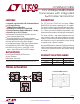

LTC2854/LTC2855
8
285455fc
For more information www.linear.com/LTC2854
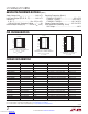
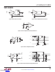
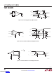
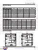
PIN FUNCTIONS
RO (Pin 1):
Receiver Output. If the receiver output is en-
abled (RE low) and A > B by 200mV, then RO will be high.
If A< B by 200mV, then RO will be low. If the receiver
inputs are open, shorted, or terminated without a signal,
RO will be high.
RE
(Pin 2): Receiver Enable. A low enables the receiver.
A high input forces the
receiver output into a high imped-
ance state.
DE (Pin 3): Driver Enable. A high on DE enables the driver.
A low input will force the driver outputs into a high imped-
ance. If
RE
is high with DE and TE low, the part will enter
a low power shutdown state.
DI (Pin 4): Driver Input. If the driver outputs are enabled
(DE high), then a low on
DI forces the driver positive out-
put low and negative output high. A high on DI, with the
driver outputs enabled, forces the driver positive output
high and negative output low.
(DD/DE/GN)
TE (Pin 5): Internal Termination Resistance Enable. A high
input will connect a termination resistor (120Ω typical)
between pins A and B.
GND (Pins 6,11/6,13/6): Ground. Pins 11 and 13 are
backside thermal pad, connected to
Ground.
Y (Pins NA/8/12): Positive Driver Output for LTC2855.
Z (Pins NA/9/13): Negative Driver Output for LTC2855.
B (Pins 9/10/14): Negative Receiver Input (and Negative
Driver Output for LTC2854).
A (Pins 8/11/15): Positive Receiver Input (and Positive
Driver Output for LTC2854).
V
CC
(Pins 10/12/16): Positive Supply. V
CC
= 3.0V < V
CC
<
3.6V. Bypass with 0.1µF ceramic capacitor.
Downloaded from Arrow.com.Downloaded from Arrow.com.Downloaded from Arrow.com.Downloaded from Arrow.com.Downloaded from Arrow.com.Downloaded from Arrow.com.Downloaded from Arrow.com.Downloaded from Arrow.com.