
Datasheet

LTC2854/LTC2855
10
285455fb
Driver
The driver provides full RS485/RS422 compatibility. When
enabled, if DI is high, Y-Z is positive for the full-duplex
device (LTC2855) and A-B is positive for the half-duplex
device (LTC2854).
When the driver is disabled, both outputs are high-
impedance. For the full-duplex LTC2855, the leakage on
the driver output pins is guaranteed to be less than 10μA
over the entire common mode range of –7V to +12V. On
the half-duplex LTC2854, the impedance is dominated by
the receiver input resistance, R
IN
.
Driver Overvoltage and Overcurrent Protection
The driver outputs are protected from short-circuits to
any voltage within the Absolute Maximum range of (V
CC
–15V) to +15V. The typical peak current in this condition
does not exceed 180mA.
If a high driver output is shorted to a voltage just above
V
CC
, a reverse current will fl ow into the supply. When this
voltage exceeds V
CC
by about 1.4V, the reverse current turns
off. Preventing the driver from turning off with outputs
shorted to output voltages just above V
CC
keeps the driver
active even for receiver loads that have a positive common
mode with respect to the driver — a valid condition.
The worst-case peak reverse short-circuit current can be as
high as 300mA in extreme cold conditions. If this current
cannot be absorbed by the supply, a 3.6V Zener diode can
be added in parallel with the supply to sink this current.
All devices also feature thermal shutdown protection that
disables the driver and receiver in case of excessive power
dissipation (see Note 4).
Receiver and Failsafe
With the receiver enabled, when the absolute value of the
differential voltage between the A and B pins is greater than
200mV, the state of RO will refl ect the polarity of (A-B).
The LTC2854/LTC2855 have a failsafe feature that guaran-
tees the receiver output to be in a logic-high state when
the inputs are either shorted, left open, or terminated
(externally or internally), but not driven. This failsafe fea-
ture is guaranteed to work for inputs spanning the entire
common mode range of –7V to +12V.
The receiver output is internally driven high (to V
CC
) or
low (to ground) with no external pull-up needed. When
the receiver is disabled the RO pin becomes high-Z with
leakage of less than ±1μA for voltages within the supply
range.
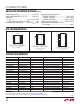
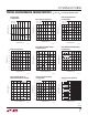
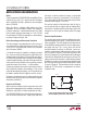
Receiver Input Resistance
The receiver input resistance from A or B to ground is guar-
anteed to be greater than 96k (C, I-Grade) when the termi-
nation is disabled. This is 8X higher than the requirements
for the RS485 standard and thus this receiver represents a
one-eighth unit load. This, in turn, means that 8X the
standard number of receivers, or 256 total, can be con-
nected to a line without loading it beyond what is called
out in the RS485 standard. The receiver input resistance
from A or B to ground on high temperature H-Grade parts
is greater than 48k providing a one-quarter unit load. The
input resistance of the receivers is unaffected by enabling/
disabling the receiver and by powering/unpowering the
part. The equivalent input resistance looking into A and B
is shown in Figure 9. The termination resistor cannot be
enabled by TE if the device is unpowered or in thermal
shutdown mode.
60Ω
60Ω
A
TE
B
285455 F09
>96kΩ
>96kΩ
Figure 9. Equivalent Input Resistance into A and B
(on the LTC2854, Valid if Driver is Disabled)
APPLICATIONS INFORMATION