
Datasheet


LTC2856-1/LTC2856-2
LTC2857-1/LTC2857-2
LTC2858-1/LTC2858-2
10
285678ff
For more information www.linear.com/LTC2856-1
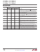
pin FuncTions
PIN NAME
PIN NUMBER
DESCRIPTION
LTC
2856-1
LTC2856-2
LTC2857-1
LTC2857-2
LTC2858-1
LTC2858-2
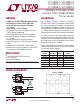
RO 1 2 1 Receiver Output. If the receiver output is enabled (RE low) and A > B by 200mV,
then RO will be high. If A < B by 200mV, then RO will be low. If the receiver
inputs are open, shorted or terminated without a valid signal, RO will be high.
RE 2 2 Receiver Enable. A low enables the receiver. A high input for
ces the receiver
output into a high impedance state.
DE 3 3 Driver Enable. A high on DE enables the driver. A low input will force the driver
outputs into a high impedance. If RE is high with DE low, the part will enter a
low power shutdown state.
DI 4 3 4 Driver Input. If the driver outputs are enabled (DE high), then a low on DI forces
the driver positive output low and negative output high. A high on DI, with
the driver outputs enabled, forces the driver positive output high and negative
output low.
GND 5/9* 4/9* 5/11* Ground. *The Exposed Pad on the DFN packages should be connected to
ground.
Y 5 6 Noninverting Driver Output for the LTC2857-1, LTC2857-2, LTC2858-1 and
LTC2858-2. High impedance when the driver is disabled (LTC2858-1) or
unpowered.
Z 6 7 Inverting Driver Output for the LTC2857-1, LTC2857-2, LTC2858-1 and
LTC2858-2. High impedance when the driver is disabled (LTC2858-1) or
unpowered.
B 7 7 8 Inverting Receiver Input (and Inverting Driver Output for the LTC2856-1 and
LTC2856-2). Impedance is > 96k
Ω in receive mode or unpowered.
A 6 8 9 Noninverting Receiver Input (and Noninverting Driver Output for the LTC2856-1
and LTC2856-2). Impedance is > 96kΩ in receive mode or unpowered.
V
CC
8 1 10 Positive Supply. 4.5V < V
CC
< 5.5V. Bypass with a 0.1µF ceramic capacitor.