
Datasheet


LTC2856-1/LTC2856-2
LTC2857-1/LTC2857-2
LTC2858-1/LTC2858-2
6
285678ff
For more information www.linear.com/LTC2856-1
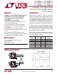
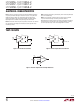
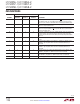
TesT circuiTs
–
+
DRIVER
DI
GND
OR
V
CC
R
285678 F01
Y
Z
R
V
OC
–
+
V
OD
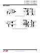
Figure 1. Driver DC Characteristics Figure 2. Driver Output Short-Circuit Current
DRIVER
DI
GND
OR
V
CC
285678 F02
Y
Z
+
–
I
OSD
–7V TO +12V
+
–
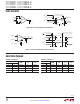
RECEIVER
285678 F03
A OR B
V
IN
I
IN
B OR A
V
IN
I
IN
R
IN
=
Figure 3. Receiver Input Current and Input Resistance
Note 1: Stresses beyond those listed under Absolute Maximum Ratings
may cause permanent damage to the device. Exposure to any Absolute
Maximum Rating condition for extended periods may affect device
reliability and lifetime. High temperatures degrade operating lifetimes.
Operating lifetime is derated at temperatures greater than 105°C.
Note 2: All currents into device pins are positive; all currents out of device
pins are negative. All voltages are referenced to device ground unless
otherwise specified.
Note 3: Maximum data rate is guaranteed by other measured parameters
and is not tested directly.
Note 4: This IC includes overtemperature protection that is intended
to protect the device during momentary overload conditions.
Overtemperature protection actives at a junction temperature exceeding
150°C. Continuous operation above the specified maximum operating
junction temperature may result in device degradation or failure.
elecTrical characTerisTics