
Datasheet


LTC2862/LTC2863/
LTC2864/LTC2865
15
2862345f
provided they are used in a network of transceivers with
similar internal failsafe features. The LTC2862-LTC2865
transceivers will operate correctly on biased, unbiased,
or under-biased networks.
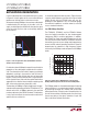
Hi-Z State
The receiver output is internally driven high (to V
CC
or V
L
)
or low (to GND) with no external pull-up needed. When the
receiver is disabled the RO pin becomes Hi-Z with leakage
of less than ±5A for voltages within the supply range.
High Receiver Input Resistance
The receiver input load from A or B to GND for the LTC2863,
LTC2864, and LTC2865 is less than one-eighth unit load,
permitting a total of 256 receivers per system without
exceeding the RS485 receiver loading specification. All
grades of the LTC2862 and the H-grade devices of the
LTC2863, LTC2864, and LTC2865 have an input load less
than one-seventh unit load over the complete tempera-
ture range of –40°C to 125°C. The increased input load
specification for these devices is due to increased junction
leakage at high temperature and the transmitter circuitry
sharing the A and B pins on the LTC2862. The input load
of the receiver is unaffected by enabling/disabling the
receiver or by powering/unpowering the part.
Supply Current
The unloaded static supply currents in these devices are
low —typically 900A for non slew limited devices and
3.3mA for slew limited devices. In applications with resis-
tively terminated cables, the supply current is dominated
by the driver load. For example, when using two 120Ω
terminators with a differential driver output voltage of
2V, the DC load current is 33mA, which is sourced by the
positive voltage supply. Power supply current increases
with toggling data due to capacitive loading and this term
can increase significantly at high data rates. A plot of the
supply current vs data rate is shown in the Typical Per-
formance Characteristics of this data sheet.
During fault conditions with a positive voltage larger than
the supply voltage applied to the transmitter pins, or dur-
ing transmitter operation with a high positive common
mode voltage, positive current of up to 80mA may flow
from the transmitter pins back to V
CC
. If the system power
supply or loading cannot sink this excess current, a 5.6V
1W 1N4734 Zener diode may be placed between V
CC
and
GND to prevent an overvoltage condition on V
CC
.
There are no power-up sequence restrictions on the
LTC2865. However, correct operation is not guaranteed for
V
L
> V
CC
.
High Speed Considerations
A ground plane layout with a 0.1µF bypass capacitor placed
less than 7mm away from the V
CC
pin is recommended. The
PC board traces connected to signals A/B and Z/Y should
be symmetrical and as short as possible to maintain good
differential signal integrity. To minimize capacitive effects,
the differential signals should be separated by more than
the width of a trace and should not be routed on top of
each other if they are on different signal planes.
Care should be taken to route outputs away from any
sensitive inputs to reduce feedback effects that might
cause noise, jitter, or even oscillations. For example, in
the full-duplex devices, DI and A/B should not be routed
near the driver or receiver outputs.
The logic inputs have a typical hysteresis of 100mV to
provide noise immunity. Fast edges on the outputs can
cause glitches in the ground and power supplies which are
exacerbated by capacitive loading. If a logic input is held
near its threshold (typically V
CC
/2 or V
L
/2), a noise glitch
from a driver transition may exceed the hysteresis levels
on the logic and data input pins, causing an unintended
state change. This can be avoided by maintaining normal
logic levels on the pins and by slewing inputs faster than
1V/s. Good supply decoupling and proper driver termi-
nation also reduce glitches caused by driver transitions.
RS485 Cable Length vs Data Rate
Many factors contribute to the maximum cable length
that can be used for RS485 or RS422 communication,
including driver transition times, receiver threshold, duty
cycle distortion, cable properties and data rate. A typical
APPLICATIONS INFORMATION