
Datasheet

LTC2862/LTC2863/
LTC2864/LTC2865
9
2862345f
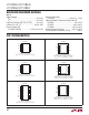
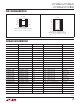
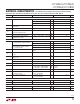
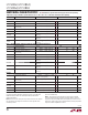
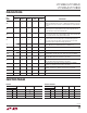
PIN FUNCTIONS
PIN
NAME
PIN NUMBER
DESCRIPTION
LTC2862 LTC2863
LTC2864
(DFN)
LTC2864
(SO) LTC2865
RO 1 2 1 2 1
Receiver Output. If the receiver output is enabled (RE low) and A–B >
200mV, then RO will be high. If A–B < –200mV, then RO will be low. If the
receiver inputs are open, shorted, or terminated without a signal, RO will
be high.
RE 2-232
Receiver Enable. A low input enables the receiver. A high input forces the
receiver output into a high impedance state. If RE is high with DE low,
the part will enter a low power shutdown state.
DE 3 - 3 4 3
Driver Enable. A high input on DE enables the driver. A low input will
force the driver outputs into a high impedance state. If DE is low with RE
high, the part will enter a low power shutdown state.
DI 4 3 4 5 4
Driver Input. If the driver outputs are enabled (DE high), then a low on
DI forces the driver noninverting output Y low and inverting output Z
high. A high on DI, with the driver outputs enabled, forces the driver
noninverting output Y high and inverting output Z low.
V
L
----5
Logic Supply: 1.65V ≤ V
L
≤ V
CC
. Bypass with 0.1µF ceramic capacitor.
Powers RO, RE, DE, DI and SLO interfaces on LTC2865 only.
GND 5 4 5 6, 7 6 Ground.
Exposed Pad 9 9 11 - 13 Connect the exposed pads on the DFN and MSOP packages to GND
SLO ----7
Slow Mode Enable. A low input switches the transmitter to the slew rate
limited 250kbps max data rate mode. A high input supports 20Mbps.
Y-5698
Noninverting Driver Output for LTC2863, LTC2864, LTC2865.
High-impedance when driver disabled or unpowered.
Z - 6 7 10 9
Inverting Driver Output for LTC2863, LTC2864, LTC2865.
High-impedance when driver disabled or unpowered.
B 7 7 8 11 10
Inverting Receiver Input (and Inverting Driver Output for LTC2862).
Impedance is > 96k in receive mode or unpowered.
A 6 8 9 12 11
Noninverting Receiver Input (and Noninverting Driver Output for
LTC2862). Impedance is > 96k in receive mode or unpowered.
V
CC
8 1 10 14 12 Power Supply. 3V < V
CC
< 5.5V. Bypass with 0.1µF ceramic capacitor to
GND.
NC 1, 8, 13 Unconnected Pins. Float or connect to GND.
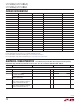
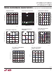
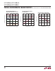
LTC2862
LOGIC INPUTS MODE A, B RO
DE RE
0 0 Receive R
IN
Active
0 1 Shutdown R
IN
High-Z
1 0 Transceive Active Active
1 1 Transmit Active High-Z
LTC2864, LTC2865:
LOGIC INPUTS MODE A, B Y, Z RO
DE RE
0 0 Receive R
IN
High-Z Active
0 1 Shutdown R
IN
High-Z High-Z
1 0 Transceive R
IN
Active Active
1 1 Transmit R
IN
Active High-Z
FUNCTION TABLES