
Datasheet
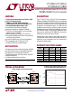


LTC2862/LTC2863/
LTC2864/LTC2865
8
2862345fc
For more information www.linear.com/LTC2862
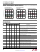
pin FuncTions
PIN
NAME
PIN NUMBER
DESCRIPTION
LTC2862
LTC2863
LTC2864
(DFN)
LTC2864
(SO)
LTC2865
RO 1
2 1 2 1 Receiver Output. If the receiver output is enabled (RE low) and A–B > 200mV,
then RO will be high. If A–B < –200mV, then RO will be low. If the receiver
inputs are open, shorted, or terminated without a signal, RO will be high.
RE 2 - 2 3 2 Receiver Enable. A low input enables the receiver. A high input forces the
receiver output into a high impedance state. If RE is high with DE low, the part
will enter a low power shutdown state.
DE 3 - 3 4 3 Driver Enable. A high input on DE enables the driver. A low input will force the
driver outputs into a high impedance state. If DE is low with RE high, the part
will enter a low power shutdown state.
DI 4 3 4 5 4 Driver Input. If the driver outputs are enabled (DE high), then a low on DI
forces the driver noninverting output Y low and inverting output Z high. A high
on DI, with the driver outputs enabled, forces the driver noninverting output Y
high and inverting output Z low.
V
L
- - - - 5 Logic Supply: 1.65V ≤ V
L
≤ V
CC
. Bypass with 0.1µF ceramic capacitor. Powers
RO, RE, DE, DI and SLO interfaces on LTC2865 only.
GND 5 4 5 6, 7 6 Ground.
Exposed Pad 9 9 11 - 13 Connect the exposed pads on the DFN and MSOP packages to GND
SLO - - - - 7 Slow Mode Enable. A low input switches the transmitter to the slew rate
limited 250kbps max data rate mode. A high input supports 20Mbps.
Y - 5 6 9 8 Noninverting Driver Output for LTC2863, LTC2864, LTC2865.
High-impedance when driver disabled or unpowered.
Z - 6 7 10 9 Inverting Driver Output for LTC2863, LTC2864, LTC2865.
High-impedance when driver disabled or unpowered.
B 7
7 8 11 10 Inverting Receiver Input (and Inverting Driver Output for LTC2862).
Impedance is > 96kΩ in receive mode or unpowered.
A 6
8 9 12 11 Noninverting Receiver Input (and Noninverting Driver Output for LTC2862).
Impedance is > 96kΩ in receive mode or unpowered.
V
CC
8 1 10 14 12 Power Supply. 3V < V
CC
< 5.5V. Bypass with 0.1µF ceramic capacitor to GND.
NC 1, 8, 13 Unconnected Pins. Float or connect to GND.
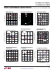
Receiver Output Voltage vs
Output Current (Source and Sink)
Receiver Propagation Delay
vs Temperature Receiver Skew vs Temperature
Typical perForMance characTerisTics
T
A
= 25°C, V
CC
= V
L
= 3.3V, unless otherwise noted.
OUTPUT CURRENT (ABSOLUTE VALUE) (mA)
0.0
0.0
RECEIVER OUTPUT VOLTAGE (V)
3.0
2.0
1.0
4.0
5.0
6.0
2.0
4.0 6.0
2862345 G10
8.0
V
L
= 5.5V
V
L
= 3.3V
V
L
= 2.25V
V
L
= 1.65V
V
L
= 1.65V TO 5.5V
TEMPERATURE (°C)
–50
46
RECEIVER DELAY (ns)
52
50
48
54
56
58
0
50 100
2862345 G11
150
V
AB
= 1.5V
C
L
= 15pF
TEMPERATURE (°C)
–50
–2.6
RECEIVER SKEW (ns)
–2.2
–2.4
–2.0
–1.8
–1.6
0
50 100
2862345 G12
150
V
AB
= 1.5V
C
L
= 15pF