
Datasheet


LTC2862/LTC2863/
LTC2864/LTC2865
6
2862345fc
For more information www.linear.com/LTC2862
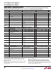
SYMBOL PARAMETER CONDITIONS MIN TYP MAX UNITS
Driver – High Speed (LTC2862-1, LTC2863-1, LTC2864-1, LTC2865 with SLO High)
f
MAX
Maximum Data Rate (Note 3)
l
20 Mbps
t
PLHD
, t
PHLD
Driver Input to Output R
DIFF
= 54Ω, C
L
= 100pF (Figure 4)
l
25 50 ns
Δt
PD
Driver Input to Output Difference
|t
PLHD
– t
PHLD
|
R
DIFF
= 54Ω, C
L
= 100pF (Figure 4)
l
2 9 ns
t
SKEWD
Driver Output Y to Output Z R
DIFF
= 54Ω, C
L
= 100pF (Figure 4)
l
±10 ns
t
RD
, t
FD
Driver Rise or Fall Time R
DIFF
= 54Ω, C
L
= 100pF (Figure 4)
l
4 15 ns
t
ZLD
, t
ZHD
,
t
LZD
, t
HZD
Driver Enable or Disable Time R
L
= 500Ω, C
L
= 50pF, RE = 0V
(Figure 5)
l
180 ns
t
ZHSD
, t
ZLSD
Driver Enable from Shutdown R
L
=500Ω, C
L
= 50pF, RE = High
(Figure 5)
l
9 µs
t
SHDND
Time to Shutdown R
L
= 500Ω, C
L
= 50pF, RE = High
(Figure 5)
l
180 ns
Driver – Slew Rate Limited ( LTC2862-2, LTC2863-2, LTC2864-2, LTC2865 with SLO Low)
f
MAX
Maximum Data Rate (Note 3)
l
250 kbps
t
PLHD
, t
PHLD
Driver Input to Output R
DIFF
= 54Ω, C
L
= 100pF (Figure 4)
l
850 1500 ns
Δt
PD
Driver Input to Output Difference
|t
PLHD
– t
PHLD
|
R
DIFF
= 54Ω, C
L
= 100pF (Figure 4)
l
50 500 ns
t
SKEWD
Driver Output Y to Output Z R
DIFF
= 54Ω, C
L
= 100pF (Figure 4)
l
±500 ns
t
RD
, t
FD
Driver Rise or Fall Time R
DIFF
= 54Ω, C
L
=100pF (Figure 4)
l
500 800 1200 ns
t
ZLD
, t
ZHD
Driver Enable Time R
L
= 500Ω, C
L
= 50pF, RE = 0V
(Figure 5)
l
1200 ns
t
LZD
, t
HZD
Driver Disable Time R
L
= 500Ω, C
L
= 50pF, RE = 0V
(Figure 5)
l
180 ns
t
ZHSD
, t
ZLSD
Driver Enable from Shutdown R
L
= 500Ω, C
L
= 50pF, RE = High
(Figure 5)
l
10 µs
t
SHDND
Time to Shutdown R
L
=500Ω, C
L
= 50pF, RE = High
(Figure 5)
l
180 ns
Receiver
t
PLHR
, t
PHLR
Receiver Input to Output C
L
= 15pF, V
CM
= 1.5V, |V
AB
| = 1.5V,
t
R
and t
F
< 4ns (Figure 6)
l
50 65 ns
t
SKEWR
Differential Receiver Skew
|t
PLHR
– t
PHLR
|
C
L
= 15pF (Figure 6) 2 9 ns
t
RR
, t
FR
Receiver Output Rise or Fall Time C
L
= 15pF (Figure 6)
l
3 12.5 ns
t
ZLR
, t
ZHR
,
t
LZR
, t
HZR
Receiver Enable/Disable Time R
L
= 1k, C
L
= 15pF, DE = High (Figure 7)
l
40 ns
t
ZHSR
, t
ZLSR
Receiver Enable from Shutdown R
L
= 1k, C
L
= 15pF, DE = 0V, (Figure 7)
l
9 µs
t
SHDNR
Time to Shutdown R
L
= 1k, C
L
= 15pF, DE = 0V, (Figure 7)
l
100 ns
swiTchinG characTerisTics
The l denotes the specifications which apply over the full operating
temperature range, otherwise specifications are at T
A
= 25°C. V
CC
= V
L
= 3.3V unless otherwise noted. (Note 2)
Note 1. Stresses beyond those listed under Absolute Maximum Ratings
may cause permanent damage to the device. Exposure to any Absolute
Maximum Rating condition for extended periods may affect device
reliability and lifetime.
Note 2.
All currents into device pins are positive; all currents out of device
pins are negative. All voltages are referenced to device ground unless
otherwise specified.
Note 3. Maximum data rate is guaranteed by other measured parameters
and is not tested directly.
Note 4. This IC includes overtemperature protection that is intended
to protect the device during momentary overload conditions. Junction
temperature will exceed 150ºC when overtemperature protection is active.
Continuous operation above the specified maximum operating temperature
may result in device degradation or failure.