
Datasheet


LTC2862/LTC2863/
LTC2864/LTC2865
13
2862345fc
For more information www.linear.com/LTC2862
applicaTions inForMaTion
Full Failsafe Operation
When the absolute value of the differential voltage between
the A and B pins is greater than 200mV with the receiver
enabled, the state of RO will reflect the polarity of (A–B).
These parts have a failsafe feature that guarantees the
receiver output will be in a logic 1 state (the idle state)
when the inputs are shorted, left open, or terminated but
not driven, for more than about 3µs. The delay allows
normal data signals to transition through the threshold
region without being interpreted as a failsafe condition. This
failsafe feature is guaranteed to work for inputs spanning
the entire common mode range of –25V to 25V.
Most competing devices achieve the failsafe function by a
simple negative offset of the input threshold voltage. This
causes the receiver to interpret a zero differential voltage
as a logic 1 state. The disadvantage of this approach is
the input offset can introduce duty cycle asymmetry at the
receiver output that becomes increasingly worse with low
input signal levels and slow input edge rates.
Other competing devices use internal biasing resistors to
create a positive bias at the receiver inputs in the absence
of an external signal. This
type of failsafe biasing is
ineffective if the network lines are shorted, or if the network
is terminated but not driven by an active transmitter.
the positive and negative thresholds. If this condition
persists for more than about 3µs the failsafe condition is
asserted and the RO pin is forced to the logic 1 state. This
circuit provides full failsafe operation with no negative
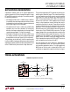
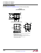
impact to receiver duty cycle symmetry, as shown in
Figure 8. The input signal in Figure 8 was obtained by
driving a 10Mbps RS485 signal through 1000 feet of cable,
thereby attenuating it to a ±200mV signal with slow rise
and fall times. Good duty cycle symmetry is observed at
RO despite the degraded input signal.
Enhanced Receiver Noise Immunity
An additional benefit of the fully symmetric receiver
thresholds is enhanced receiver noise immunity. The
differential input signal must go above the positive
threshold to register as a logic 1 and go below the
negative threshold to register as a logic 0. This provides
a hysteresis of 150mV (typical) at the receiver inputs for
any valid data signal. (An invalid data condition such as
a DC sweep of the receiver inputs will produce a different
observed hysteresis due to the activation of the
failsafe
circuit.)
Competing devices that employ a negative offset
of the input threshold voltage generally have a much
smaller hysteresis and subsequently have lower receiver
noise immunity.
RS485 Network Biasing
RS485 networks are usually biased with a resistive divider
to generate a differential voltage of ≥200mV on the data
lines, which establishes a logic 1 state (the idle state)
when all the transmitters on the network are disabled. The
values of the biasing resistors are not fixed, but depend
on the number and type of transceivers on the line and
the number and value of terminating resistors. Therefore,
the values of the biasing resistors must be customized to
each specific network installation, and may change if nodes
are added to or removed from the network.
The internal failsafe feature of the LTC2862-LTC2865
eliminates the need for external network biasing resistors
provided they are used in a network of transceivers with
similar internal failsafe features. The LTC2862-LTC2865
transceivers will operate correctly on biased, unbiased,
or under-biased networks.
Figure 8. Duty Cycle of Balanced Receiver with ±200mV
10Mbps Input Signal
A, B
200mV/DIV
A–B
200mV/DIV
40ns/DIV
2862345 F08
RO
1.6V/DIV
The LTC2862 series uses fully symmetric positive and
negative receiver thresholds (typically ±75mV) to maintain
good duty cycle symmetry at low signal levels. The failsafe
operation is performed with a window comparator to
determine when the differential input voltage falls between