
Datasheet


LTC2862/LTC2863/
LTC2864/LTC2865
17
2862345fc
For more information www.linear.com/LTC2862
applicaTions inForMaTion
A protection network shown in the Typical Applications
section (network for IEC level 4 protection against surge,
EFT and ESD) meets this challenge. The network provides
the following protection:
• IEC 61000-4-2 ESD Level 4: ±30KV contact, ±30kV air
(line to GND, direct discharge to bus pins with transceiver
and protection circuit mounted on a ground referenced
test card per Figure 4 of the standard)
• IEC 61000-4-4 EFT Level 4: ±5KV (line to GND, 5kHz
repetition rate, 15ms burst duration, 60 second test
duration, discharge coupled to bus pins through 100pF
capacitor per paragraph 7.3.2 of the standard)
• IEC 61000-4-5 Surge Level 4: ±5KV (line to GND, line to
line, 8/20µs waveform, each line coupled to generator
through 80Ω resistor per Figure 14 of the standard)
This protection circuit adds only ~8pF of capacitance per
line (line to GND), thereby providing an extremely high level
of protection without significant impact to the performance
of the LTC2865 family transceivers at high data rates.
The gas discharge tubes (GDTs) provide the primary pro-
tection against electrical surges. These devices provide a
very low impedance and high current carrying capability
when they fire, safely discharging the surge current to
GND. The transient blocking units (TBUs) are solid state
devices that
switch from a low impedance pass through
state
to a high impedance current limiting state when a
specified current level is reached. These devices limit the
current and power that can pass through to the secondary
protection. The secondary protection consists of a
bidirectional thyristor, which triggers above 35V to protect
the bus pins of the LTC2865 family transceiver. The high
trigger voltage of the secondary protection maintains the
full ±25V common mode range of the receivers. The final
component of the network is the metal oxide varistors
(MOVs) which are used to clamp the voltage across the
TBUs to protect them against fast ESD and EFT transients
which exceed the turn-on time of the GDT.
The high performance of this network is attributable to
the low capacitance of the GDT and thyristor primary
and secondary protection devices. The high capacitance
MOV floats on the line and is shunted by the TBU, so it
contributes no appreciable capacitive load on the signal.
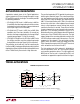
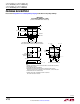
PROFIBUS Compatible Line Interface
Typical applicaTions
RO
RE
DE
DI
8.2Ω
2862345 TA02
A*
B*
* THE POLARITY OF A AND B IN THIS DATA SHEET IS OPPOSITE THE POLARITY DEFINED BY PROFIBUS.
V
CC
(4.75V TO 5.25V)
GND
LTC2862-1
8.2Ω
390Ω
4V
P-P
≤ V
OD
≤ 7V
P-P
AT 12Mbps
220Ω
390Ω
B WIRE
A WIRE
B WIRE
A WIRE
V
CC
390Ω
220Ω
390Ω
V
CC
100m
5.5Ω/WIRE
V
OD