
Datasheet


LTC2870/LTC2871
20
28701fb
For more information www.linear.com/LTC2870
Overview
The LTC2870 and LTC2871 are flexible multiprotocol
transceivers supporting RS485/RS422 and RS232 pro-
tocols. These parts can be powered from a single 3V to
5.5V supply with optional logic interface supply as low as
1.7V. An integrated DC/DC converter provides the posi-
tive and negative supply rails needed for RS232 operation.
Automatically selected integrated termination resistors
for both RS232 and RS485 protocols are included, elimi-
nating the need for external components and switching
relays. Both parts include loopback control for self-test
and debug as well as logically-switchable half- and full-
duplex control of the RS485 bus inter
face.
The LTC2870 offers a single port that can be configured
as either two RS232 receivers and drivers or one RS485/
RS422 receiver and driver depending on the state of the
485/232 pin. Control inputs DXEN and RXEN provide
independent control of driver and receiver operation for
either RS232 or RS485 transceivers, depending on the
selected operating protocol.
The LTC2871 separates the RS232 and RS485 transceiv-
ers into independent I/Os allowing simultaneous opera-
tion of two RS232 transceivers and one RS485 trans-
ceiver. Independent control over driver and receiver mode
for each protocol is provided with logic inputs DX232,
RX232, DX485, RX485. Single channel RS232 operation
is possible via the CH2 control pin. The disabled channel
maintains a Hi-Z state on the receiver input and driver
output, allowing these lines to be shared with other
transceivers.
Both parts feature rugged operation with ESD ratings
of ±26kV (LTC2870) and ±16kV (LTC2871) HBM on the
RS232 and RS485 receiver inputs and driver outputs,
both unpowered and powered. All other pins offer pro-
tection exceeding ±4kV.
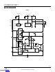
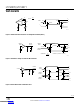
DC/DC Converter
The on-chip DC/DC converter operates from the V
CC
input,
generating a 7V V
DD
supply and a charge pumped –6.3V
V
EE
supply, as shown in Figure13. V
DD
and V
EE
power the
output stage of the RS232 drivers and are regulated to lev-
els that guarantee greater than ±5V output swing. The DC/
DC converter requires a 10µH inductor (L1) and a bypass
capacitor (C4) of 2.2µF. The charge pump capacitor (C1)
is 220nF and the storage capacitors (C2 and C3) are 1µF.
Larger storage capacitors up to 4.7µF may be used if C1
and C4 are scaled proportionately. Locate C1–C4 close to
their associated pins.
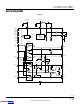
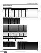
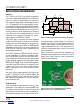
Figure14 shows the layout of external components on
the bottom of the demonstration circuit for the LTC2871
(Demo Circuit 1786A). Refer to Layout Considerations
section for further guidance.
applicaTions inForMaTion
Figure13. DC/DC Converter with Required External Components
28701 F13
BOOST
REGULATOR
V
CC
3V TO 5.5V
V
L
1.7V TO V
CC
C1
220nF
L1
10µH
C4
2.2µF
V
CC
V
DD
V
EE
SW
GND
GND
CAP
C5
0.1µF
C2
1µF
C3
1µF
V
L
Figure14. Demo Circuit 1786A (Bottom) Showing Layout of
External Devices. U.S. Penny Included for Scale
Downloaded from Arrow.com.Downloaded from Arrow.com.Downloaded from Arrow.com.Downloaded from Arrow.com.Downloaded from Arrow.com.Downloaded from Arrow.com.Downloaded from Arrow.com.Downloaded from Arrow.com.Downloaded from Arrow.com.Downloaded from Arrow.com.Downloaded from Arrow.com.Downloaded from Arrow.com.Downloaded from Arrow.com.Downloaded from Arrow.com.Downloaded from Arrow.com.Downloaded from Arrow.com.Downloaded from Arrow.com.Downloaded from Arrow.com.Downloaded from Arrow.com.Downloaded from Arrow.com.