
Datasheet

LTC2870/LTC2871
20
28701f
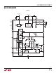
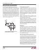
Inrush Current and Supply Overshoot Precaution
In certain applications fast supply slew rates are generated
when power is connected. If the V
CC
voltage is greater
than 4.5V and its rise time is faster than 10s, the pins
V
DD
and SW can exceed their absolute maximum values
during start-up. When supply voltage is applied to V
CC
, the
voltage difference between V
CC
and V
DD
generates inrush
current flowing through inductor L1 and capacitors C1 and
C2. The peak inrush current must not exceed 2A. To avoid
this condition, add a 1 resistor as shown in Figure 14.
This precaution is not relevant for supply voltages below
4.5V or rise times longer than 10s.
V
L
Logic Supply and Logic Pins
A separate logic supply pin V
L
allows the LTC2870 and
LTC2871 to interface with any logic signal from 1.7V to
5.5V. All logic I/Os use V
L
as their high supply. For proper
operation, V
L
should not be greater than V
CC
. During
power-up, if V
L
is higher than V
CC
, the device will not be
damaged, but behavior of the device is not guaranteed.
If V
L
is not connected to V
CC
, bypass V
L
with a 0.1µF
capacitor to GND.
RS232 and RS485 driver outputs are undriven and the
RS485 termination resistors are disabled when V
L
or V
CC
is grounded or V
CC
is disconnected.
Although all logic input pins reference V
L
as their high
supply, they can be driven up to 7V, independent of V
L
and
V
CC
, with the exception of FEN, which must not exceed V
L
by more than 1V for proper operation. Logic input pins
do not have internal biasing devices to pull them up or
down. They must be driven high or low to establish valid
logic levels; do not float.
RS485 Driver
The RS485 driver provides full RS485/RS422 compati-
bility. When enabled, if DI is high, Y – Z is positive. With
the driver disabled the Y and Z output resistance is greater
than 96k (typically 125k) to ground over the entire
common mode range of –7V to +12V. This resistance is
equivalent to the input resistance on these lines when the
driver is configured in half-duplex mode and Y and Z act
as the RS485 receiver inputs.
Driver Overvoltage and Overcurrent Protection
The RS232 and RS485 driver outputs are protected from
short circuits to any voltage within the absolute maximum
range ±15V. The maximum current in this condition is 90mA
for the RS232 driver and 250mA for the RS485 driver.
If the RS485 driver output is shorted to a voltage greater
than V
CC
, when it is active, positive current of up to 100mA
may flow from the driver output back to V
CC
. If the system
power supply or loading cannot sink this excess current,
clamp V
CC
to GND with a Zener diode (e.g., 5.6V, 1W,
1N4734) to prevent an overvoltage condition on V
CC
.
APPLICATIONS INFORMATION
Figure 14. Supply Current Overshoot Protection
for Input Supplies of 4.5V of Higher
28701 F14
0V
5V
≤10µs
C1
220nF
L1
10µH
INRUSH
CURRENT
C4
2.2µF
R1
1
1/8W
V
CC
V
DD
GND
SW CAP
C2
1µF