
Datasheet

LTC2870/LTC2871
23
28701f
APPLICATIONS INFORMATION
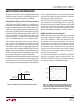
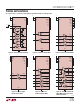
Logic Loopback
A loopback mode connects the driver inputs to the re-
ceiver outputs (non-inverting) for self test. This applies to
both RS232 and RS485 transceivers. Loopback mode is
entered when the LB pin is high and the relevant receiver
is enabled.
In loopback mode, the drivers function normally. They can
be disabled with outputs in a Hi-Z state or left enabled to
allow loopback testing in normal operation. Loopback
works in half- or full-duplex mode and does not affect the
termination resistors.
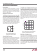
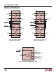
DATA RATE (bps)
CABLE LENGTH (FT)
28701 F19
10k
1k
100
10
10k 10M 100M1M100k
LTC2870/LTC2871
MAX DATA RATE
RS485/RS422
MAX DATA RATE
Figure 19. Cable Length vs Data Rate (RS485/RS422
Standard Shown in Vertical Solid Line)
The solid vertical line represents the specified maximum
data rate in the RS485/RS422 standards. The dashed lines
at 20Mbps show the maximum data rates of the LTC2870
and LTC2871.
Layout Considerations
All V
CC
pins must be connected together on the PC board
with very low impedance traces or with a dedicated plane.
A 2.2µF or larger decoupling capacitor (C4 in Figure 13)
must be placed less than 0.7cm away from the V
CC
pin
that is adjacent to the V
DD
pin.
0.1µF capacitors to GND can be added on the V
CC
pins
adjacent to the B and V
L
pins if the connection to the 2.2µF
decoupling capacitor is not direct or if the trace is very
narrow. All GND pins must be connected together and
all V
EE
pins must be connected together, including the
exposed pad on the bottom of the package. The bypass
capacitor at V
EE
, C3, should be positioned closest to the
V
EE
pin that is adjacent to the CAP pin, with no more than
1cm of total trace length between the V
EE
and GND pins.
Place the charge pump capacitor, C1, directly adjacent to
the SW and CAP pins, with no more than one centimeter
of total trace length to maintain low inductance. Close
placement of the inductor, L1, is of secondary importance
compared to the placement of C1 but should include no
more than two centimeters of total trace length.
The PC board traces connected to high speed signals A/B
and Y/Z should be symmetrical and as short as possible
to minimize capacitive imbalance and maintain good dif-
ferential signal integrity. To minimize capacitive loading
effects, the differential signals should be separated by
more than the width of a trace.
Route outputs away from sensitive inputs to reduce
feedback effects that might cause noise, jitter, or even
oscillations. For example, do not route DI or A/B near the
driver or receiver outputs.
RS485 Cable Length vs Data Rate
For a given data rate, the maximum transmission dis-
tance is bounded by the cable properties. A typical curve
of cable length vs data rate compliant with the RS485/
RS422 standards is shown in Figure 19. Three regions
of this curve reflect different performance limiting fac-
tors in data transmission. In the flat region of the curve,
maximum distance is determined by resistive losses in
the cable. The downward sloping region represents limits
in distance and data rate due to AC losses in the cable.