
Datasheet

LTC2870/LTC2871
19
28701f
Overview
The LTC2870 and LTC2871 are flexible multiprotocol trans-
ceivers supporting RS485/RS422 and RS232 protocols.
These parts can be powered from a single 3V to 5.5V
supply with optional logic interface supply as low as 1.7V.
An integrated DC/DC converter provides the positive and
negative supply rails needed for RS232 operation. Auto-
matically selected integrated termination resistors for both
RS232 and RS485 protocols are included, eliminating the
need for external components and switching relays. Both
parts include loopback control for self-test and debug as
well as logically-switchable half- and full-duplex control
of the RS485 bus interface.
The LTC2870 offers a single port that can be configured
as either two RS232 receivers and drivers or one RS485/
RS422 receiver and driver depending on the state of the
485/232 pin. Control inputs DXEN and RXEN provide
independent control of driver and receiver operation for
either RS232 or RS485 transceivers, depending on the
selected operating protocol.
The LTC2871 separates the RS232 and RS485 transceivers
into independent I/Os allowing simultaneous operation
of two RS232 transceivers and one RS485 transceiver.
Independent control over driver and receiver mode for
each protocol is provided with logic inputs DX232, RX232,
DX485, RX485. Single channel RS232 operation is possible
via the CH2 control pin. The disabled channel maintains a
Hi-Z state on the receiver input and driver output, allowing
these lines to be shared with other transceivers.
Both parts feature rugged operation with ESD ratings
of ±26kV (LTC2870) and ±16kV (LTC2871) HBM on the
RS232 and RS485 receiver inputs and driver outputs, both
unpowered and powered. All other pins offer protection
exceeding ±4kV.
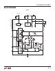
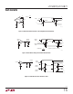
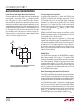
DC/DC Converter
The on-chip DC/DC converter operates from the V
CC
input,
generating a 7V V
DD
supply and a charge pumped –6.3V
V
EE
supply, as shown in Figure 13. V
DD
and V
EE
power
the output stage of the RS232 drivers and are regulated
to levels that guarantee greater than ±5V output swing.
The DC/DC converter requires a 10µH inductor (L1) and a
bypass capacitor (C4) of 2.2µF. The charge pump capacitor
(C1) is 220nF and the storage capacitors (C2 and C3) are
1µF. Larger storage capacitors up to 4.7µF may be used if
C1 and C4 are scaled proportionately. Locate C1–C4 close
to their associated pins.
Up to two LTC2870 or LTC2871 devices can be powered
from one of the devices; see Figure 48 in the Typical Ap-
plications section.
Inductor Selection
A 10H inductor with a saturation current (I
SAT
) rating
of at least 220mA and a DCR (copper wire resistance) of
less than 1.3 is required. Some small inductors meeting
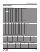
these requirements are listed in Table 12.
Table 12. Recommended Inductors
PART NUMBER
I
SAT
(mA)
MAX
DCR (Ω) SIZE(mm) MANUFACTURER
LBC2016T100K
CBC2016T100M
245
380
1.07
1.07
2 × 1.6 × 1.6
2 × 1.6 × 1.6
Taiyo Yuden
www.t-yuden.com
FSLB2520-100K 220 1.1 2.5 × 2 × 1.6 Toko
www.tokoam.com
Capacitor Selection
The small size of ceramic capacitors makes them ideal
for the LTC2870 and LTC2871. Use X5R or X7R dielectric
types; their ESR is low and they retain their capacitance
over relatively wide voltage and temperature ranges. Use
a voltage rating of at least 10V.
APPLICATIONS INFORMATION
Figure 13. DC/DC Converter
28701 F13
3V TO 5.5V
C1
220nF
L1
10µH
C4
2.2µF
V
CC
V
DD
V
EE
SW CAP
C2
1µF
C3
1µF
PULSE-SKIPPING
BOOST
REGULATOR
f = 1.2MHz