
Datasheet

LTC2870/LTC2871
9
28701f
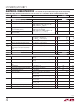
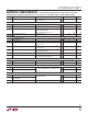
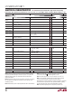
PIN FUNCTIONS
PIN NAME
LTC2870
QFN
LTC2870
TSSOP
LTC2871
QFN
LTC2871
TSSOP DESCRIPTION
V
CC
16, 20, 24 19, 23, 27 21, 27, 33 25, 31, 37 Input Supply (3V to 5.5V). Tie all three pins together and connect a 2.2µF or larger
capacitor between V
CC
(adjacent to V
DD
) and GND.
V
L
25 28 35 1 Logic Supply (1.7V to 5.5V) for the receiver outputs, driver inputs, and control inputs.
Bypass this pin to GND with a 0.1µF capacitor if not tied tot V
CC
. Keep V
L
≤ V
CC
for
proper operation. However, V
L
> V
CC
will not damage the device, provided that absolute
maximum limits are respected.
V
DD
15 18 20 24 Generated Positive Supply Voltage for RS232 Driver (+7V). Connect 1F capacitor
between V
DD
and GND.
V
EE
1, 12, 29 4, 15, 29 1, 12, 16,
19, 39
5, 16, 20,
23, 39
Generated Negative Supply Voltage for RS232 Driver (–6.3V). Tie all pins together and
connect 1F capacitor between V
EE
(adjacent to the CAP pin) and GND.
GND 10, 13,
18, 23
13, 16,
21, 26
14, 17,
25, 32
18, 21,
29, 36
Ground. Tie all four pins together.
CAP 11 14 15 19 Charge Pump Capacitor for Generated Negative Supply Voltage. Connect a 220nF
capacitor between CAP and SW.
SW 14 17 18 22 Switch Pin. Connect 10µH inductor between SW and V
CC
.
A 22 25 29 33 RS485 Positive Receiver Input (Full-Duplex Mode) or RS232 Receiver Input 1 (LTC2870).
B 21 24 28 32 RS485 Negative Receiver Input (Full-Duplex Mode) or RS232 Receiver Input 2 (LTC2870).
RA 2 5 RS485 Differential Receiver Output or RS232 Receiver Output 1.
RB 3 6 RS232 Receiver Output 2.
RO 34 38 RS485 Differential Receiver Output.
RIN1 31 35 RS232 Receiver Input 1.
RIN2 30 34 RS232 Receiver Input 2.
ROUT1 2 6 RS232 Receiver Output 1.
ROUT2 3 7 RS232 Receiver Output 2.
DIN1 8 12 RS232 Driver Input 1.
DIN2 9 13 RS232 Driver Input 2.
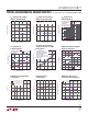
TYPICAL PERFORMANCE CHARACTERISTICS
RS232 Driver Outputs Enabling
and Disabling V
DD
and V
EE
Powering Up V
DD
and V
EE
Ripple
5V/DIV
2V/DIV
28701 G20
40µs/DIV
FEN
VDD
VEE
5V/DIV
28701 G19
40µs/DIV
TOP CURVES: FAST ENABLE j DX232
BOTTOM CURVES: SHUTDOWN j DX232
FEN = 1
FEN = 0
DOUT1
DOUT2
DOUT1
DX232
DOUT2
10mV/DIV
28701 G21
40µs/DIV
FAST ENABLE MODE,
ALL DRIVERS AND RECEIVERS DISABLED.
VDD RIPPLE
VEE RIPPLE
T
A
= 25°C, V
CC
= V
L
= 3.3V, unless otherwise noted.