
Datasheet

LTC2870/LTC2871
6
28701f
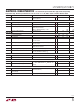
ELECTRICAL CHARACTERISTICS
The l denotes the specifications which apply over the full operating
temperature range, otherwise specifications are at T
A
= 25°C. V
CC
= V
L
= 3.3V, TE485 = 0V, LB = 0V unless otherwise noted. V
L
≤ V
CC
.
SYMBOL PARAMETER CONDITIONS MIN TYP MAX UNITS
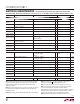
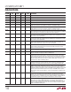
RS485 AC Characteristics
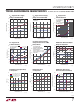
Maximum Data Rate (Note 3)
l
20 Mbps
t
PLHD485
t
PHLD485
Driver Propagation Delay R
DIFF
= 54, C
L
= 100pF (Figure 4)
l
20 70 ns
Driver Propagation Delay Difference
|t
PLHD485
– t
PHLD485
|
R
DIFF
= 54, C
L
= 100pF (Figure 4)
l
16 ns
t
SKEWD485
Driver Skew (Y to Z) R
DIFF
= 54, C
L
= 100pF (Figure 4)
l
1±6 ns
t
RD485
, t
FD485
Driver Rise or Fall Time R
DIFF
= 54, C
L
= 100pF (Figure 4)
l
15 ns
t
ZLD485
, t
ZHD485
,
t
LZD485
, t
HZD485
Driver Output Enable or Disable Time FEN = V
L
, R
L
= 500, C
L
= 50pF (Figure 5)
l
120 ns
t
ZHSD485
, t
ZLSD485
Driver Enable from Shutdown R
L
= 500, C
L
= 50pF (Figure 5)
l
8µs
t
PLHR485
, t
PHLR485
Receiver Input to Output C
L
= 15pF, V
CM
= 1.5V, |A – B| = 1.5V
(Figure 6) (Note 5)
l
65 85 ns
t
SKEWR485
Differential Receiver Skew
|t
PLHR485
– t
PHLR485
|
C
L
= 15pF (Figure 6)
l
16 ns
t
RR485
, t
FR485
Receiver Output Rise or Fall Time C
L
= 15pF (Figure 6)
l
315 ns
t
ZLR485
, t
ZHR485
,
t
LZR485
, t
HZR485
Receiver Output Enable or Disable Time FEN = V
L
, R
L
= 1k, C
L
= 15pF (Figure 7)
l
50 ns
t
RTEN485
, t
RTZ485
Termination Enable or Disable Time FEN = V
L
, V
B
= 0V, V
AB
= 2V (Figure 8) (Note 5)
l
100 µs
RS232 AC Characteristics
Maximum Data Rate R
L
= 3k, C
L
= 2500pF
R
L
= 3k, C
L
= 500pF
(Note 3)
l
l
100
500
kbps
kbps
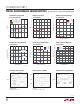
Driver Slew Rate (Figure 9) R
L
= 3k, C
L
= 2500pF
R
L
= 3k, C
L
= 50pF
l
l
4
30
V/µs
V/µs
t
PHLD232
, t
PLHD232
Driver Propagation Delay R
L
= 3k, C
L
= 50pF (Figure 9)
l
12 µs
t
SKEWD232
Driver Skew R
L
= 3k, C
L
= 50pF (Figure 9) 50 ns
t
ZLD232
, t
ZHD232
,
t
LZD232
, t
HZD232
Driver Output Enable or Disable Time FEN = V
L
, R
L
= 3k, C
L
= 50pF (Figure 10)
l
0.4 2 µs
t
PHLR232
, t
PLHR232
Receiver Propagation Delay C
L
= 150pF (Figure 11)
l
60 200 ns
t
SKEWR232
Receiver Skew C
L
= 150pF (Figure 11) 25 ns
t
RR232
, t
FR232
Receiver Rise or Fall Time C
L
= 150pF (Figure 11)
l
60 200 ns
t
ZLR232
, t
ZHR232
,
t
LZR232
, t
HZR232
Receiver Output Enable or Disable Time FEN = V
L
, R
L
= 1k, C
L
= 150pF (Figure 12)
l
0.7 2 µs
Power Supply Generator
V
DD
/V
EE
Supply Rise Time
FEN =
, (Notes 3 and 4)
l
0.2 2 ms
Note 1: Stresses beyond those listed under Absolute Maximum Ratings
may cause permanent damage to the device. Exposure to any Absolute
Maximum Rating condition for extended periods may affect device
reliability and lifetime.
Note 2: All currents into device pins are positive; all currents out of device
pins are negative. All voltages are referenced to device ground unless
otherwise specified.
Note 3: Guaranteed by other measured parameters and not tested directly.
Note 4: Time from FEN
until V
DD
≥ 5V and V
EE
≤ –5V. External
components as shown in the Typical Application section.
Note 5: Condition applies to A, B for H/F = 0V, and Y, Z for H/F = V
L
.
Note 6: This IC includes overtemperature protection that is intended
to protect the device during momentary overload conditions.
Overtemperature protection activates at a junction temperature exceeding
150°C. Continuous operation above the specified maximum operating
junction temperature may result in device degradation or failure.
Note 7: Guaranteed by design and not subject to production test.