
Datasheet


LTC2872
21
2872f
applicaTions inForMaTion
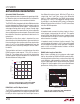
At frequencies below 100kbps, the maximum cable length
is determined by DC resistance in the cable. In this ex-
ample, a cable longer than 4000ft will attenuate the signal
at the far end to less than what can be reliably detected
by the receiver.
For data rates above 100kbps, the capacitive and inductive
properties of the cable begin to dominate this relation-
ship. The attenuation of the cable is frequency and length
dependent, resulting in increased rise and fall times at
the far end of the cable. At high data rates or long cable
lengths, these transition times become a significant part
of the signal bit time. Jitter and intersymbol interference
aggravate this so that the time window for capturing valid
data at the receiver becomes impossibly small.
The boundary at 20Mbps in Figure 19 represents the
guaranteed maximum operating rate of the LTC2872. The
dashed vertical line at 10Mbps represents the specified
maximum data rate in the RS485 standard. This boundary
is not a limit, but reflects the maximum data rate that the
specification was written for.
It should be emphasized that the plot in Figure 19 shows
a typical relation between maximum data rate and cable
length. Results with the LTC2872 will vary, depending on
cable properties such as conductor gauge, characteristic
impedance, insulation material, and solid versus stranded
conductors.
Layout Considerations
All V
CC
pins must be connected together and all ground
pins must be connected together on the PC board with
very low impedance traces or dedicated planes. A 2.2µF,
or larger, bypass capacitor should be placed less than
0.7cm away from V
CC
Pin 21. This V
CC
pin, as well as GND
Pin 18, mainly service the DC/DC converter. Additional
bypass capacitors of 0.1µF or larger, can be added to V
CC
Pins 1 and 31 if the traces back to the 2.2µF capacitor
are indirect or narrow. These V
CC
pins mainly service the
transceivers #1 and #2, respectively. Table 11 summarizes
the bypass capacitor requirements. The capacitors listed
in the table should be placed closest to their respective
supply and ground pin.
Table 11. Bypass Capacitor Requirements
CAPACITOR SUPPLY (PIN) RETURN (PIN) COMMENT
2.2µF V
CC
(21) GND (18) Required
2.2 µF V
DD
(20) GND (18) Required
2.2uF V
EE
(39) GND (18) Required
0.1µF V
L
(35) GND (34) Required*
0.1µF V
CC
(1) GND (5) Optional
0.1µF V
CC
(31) GND (27) Optional
* If V
L
is not connected to V
CC
.
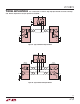
Place the charge pump capacitor, C1, directly adjacent to
the SW and CAP pins, with no more than one centimeter
of total trace length to maintain low inductance. Close
placement of the inductor, L1, is of secondary importance
compared to the placement of C1 but should include no
more than two centimeters of total trace length.
The PC board traces connected to high speed signals A/B
and Y/Z should be symmetrical and as short as possible
to minimize capacitive imbalance and to maintain good
differential signal integrity. To minimize capacitive loading
effects, the differential signals should be separated by
more than the width of a trace and should not be routed
on top of each other if they are on different signal planes.
Care should be taken to route outputs away from any sen-
sitive inputs to reduce feedback effects that might cause
noise, jitter, or even oscillations. For example, DI and A/B
should not be routed near the driver or receiver outputs.