
Datasheet


LTC2872
22
2872f
Typical applicaTions
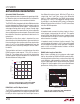
Figure 20. LTC2872 in Various Basic Port Configurations
Figure 21. Loopback in
RS232 and RS485 Modes
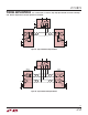
Figure 22. Half-Duplex RS485
Mode with Driver and Receiver Line
Termination on Each Port
Figure 23. Full-Duplex RS485 Mode
with Driver and Receiver Line
Termination on Port 1, and Receiver-
Only Termination on Port 2
V
L
DY1
DZ1
Y1
Z1
RA1
RB1
A1
B1
DY2
Y2
Z2
RA2
A2
B2
2872 F21
LTC2872
LB
485/232_2
485/232_1
RXEN1
RXEN2
H/F
GND
V
L
2872 F22
LTC2872
H/F
TE485_1
TE485_2
485/232_1
485/232_2
DZ1
DZ2
LB
GND
DY1
120Ω
Y1
Z1
RA1
A1
B1
120Ω
DY2
120Ω
Y2
Z2
RA2
A2
B2
120Ω
V
L
2872 F23
LTC2872
TE485_1
TE485_2
DZ1
485/232_1
485/232_2
DZ2
H/F
LB
GND
DY2
Y2
Z2
RA2
A2
B2
120Ω
DY1
Y1
Z1
RA1
A1
B1
120Ω
120Ω
V
CC
= 3V to 5.5V, V
L
= 1.7V to V
CC
. Logic input pins not shown are tied to a valid logic
state. External components necessary for operation are not shown.
2872 F20
485/232_1
485/232_2
LB
DY1
DZ1
Y1
Z1
RA1
RB1
A1
B1
DY2
DZ2
Y2
Z2
RA2
RB2
A2
B2
LTC2872
PORT 1: RS232
PORT 2: RS232
PORT 1: RS232
PORT 2: RS485
PORT 1: RS485
PORT 2: RS232
PORT 1: RS485
PORT 2: RS485
DY1
DZ1
Y1
Z1
RA1
RB1
A1
B1
DY2
Y2
Z2
RA2
A2
B2
LTC2872
485/232_2 485/232_1
H/F
LB
GND
DY2
DZ2
Y2
Z2
RA2
RB2
A2
B2
DY1
Y1
Z1
RB1
A1
B1
LTC2872
485/232_1 485/232_2
H/F
LB
GND
DY1
V
L
V
L
V
L
Y1
Z1
RA1
A1
B1
LTC2872
485/232_1
485/232_2
H/F
LB
GND
DY2
Y2
Z2
RA2
A2
B2