
Datasheet


LTC2909
8
2909fb
APPLICATIO S I FOR ATIO
WUU
U
The LTC2909 is a low power, high accuracy dual/triple
supply monitor with two adjustable inputs and an ac-
curate UVLO. Reset timeout may be selected with an
external capacitor, set to an internally generated 200ms,
or disabled entirely.
The three-state polarity select pin (SEL) chooses one of
three possible polarity combinations for the adjustable input
thresholds, as described in Table 1. Both input voltages
(V
ADJ1
and V
ADJ2
) must be valid (above threshold if con-
fi gured for positive polarity, below threshold if confi gured
for negative polarity), and V
CC
above the UVLO threshold
for the reset timeout before
⎯
R
⎯
S
⎯
T is released. The LTC2909
asserts the reset output during power-up, power-down and
brownout conditions on any of the voltage inputs.
Power-Up
The LTC2909 uses proprietary low voltage drive circuitry
for the
⎯
R
⎯
S
⎯
T pin which holds
⎯
R
⎯
S
⎯
T low with as little as
200mV of V
CC
. This helps prevent an unknown voltage
on the
⎯
R
⎯
S
⎯
T line during power-up.
In applications where the low voltage pull-down capabil-
ity is important, the supply to which the external pull-up
resistor connects should be the same supply which powers
the part. Using the same supply for both ensures that
⎯
R
⎯
S
⎯
T
never fl oats above 200mV during power-up, as the pull-
down ability of the pin will then increase as the required
pull-down current to maintain a logic low increases.
Once V
CC
passes the UVLO threshold, polarity selection
and timer initialization will occur. If the monitored supplies
(ADJ1 and ADJ2) are valid, the appropriate timeout delay
will begin, after which
⎯
R
⎯
S
⎯
T will be released. Otherwise, the
part will wait until all supplies are valid (including V
CC
above
the UVLO threshold) before beginning the timeout.
Power-Down
On power-down, once V
CC
drops below the UVLO threshold
or either V
ADJ
becomes invalid,
⎯
R
⎯
S
⎯
T asserts logic low. V
CC
of at least 0.5V guarantees a logic low of 0.15V at
⎯
R
⎯
S
⎯
T.
Shunt Regulator
The LTC2909 contains an internal 6.5V shunt regulator on
the V
CC
pin to allow operation from a high voltage supply. To
operate the part from a supply higher than 6V, the V
CC
pin
must have a series resistor, R
CC
, to the supply. This resistor
should be sized according to the following equation:
VV
mA
R
VV
µA I
SMAX
CC
SMIN
VRE
() ()
–. –.62
10
68
200
≤≤
+
FF
where V
S(MIN)
and V
S(MAX)
are the operating minimum and
maximum of the supply, and I
VREF
is the maximum current
the user expects to draw from the reference output.
As an example, consider operation from an automobile bat-
tery which might dip as low as 10V or spike to 60V. Assume
that the user will be drawing 100A from the reference. We
must then pick a resistance between 5.4k and 10.7k.
When the V
CC
pin is connected to a low impedance supply,
it is important that the supply voltage never exceed 6V,
or the shunt regulator may begin to draw large currents.
Some supplies may have nominal value suffi ciently close
to the shunt regulation voltage to prevent sizing of the
resistor according to the above equation. For such sup-
plies, a 470Ω series resistor may be used.
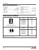
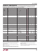
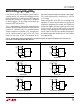
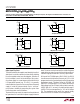
Polarity Selection
The external connection of the SEL pin selects the polarities
of the LTC2909 adjustable inputs. SEL may be connected to
GND, connected to V
CC
or left unconnected during normal
operation. When left unconnected, the maximum leakage
allowable from the pin to either GND or V
CC
is 10A. Table 1
shows the three possible selections of polarity based on
SEL connection.
Table 1. Voltage Threshold Selection
ADJ1 INPUT ADJ2 INPUT SEL
Positive Polarity
(+) UV or (–) OV
Positive Polarity
(+) UV or (–) OV
V
CC
Positive Polarity
(+) UV or (–) OV
Negative Polarity
(–) UV or (+) OV
Open
Negative Polarity
(–) UV or (+) OV
Negative Polarity
(–) UV or (+) OV
Ground
Note: Open = open circuit or driven by a three-state buffer in high impedance
state with leakage current less than 10A.
If the user’s application requires, the SEL pin may be driven
using a three-state buffer which satisfi es the V
IL
, V
IH
and
leakage of the three-state pin.