
Datasheet

LTC2912
6
2912fb
For more information www.linear.com/LTC2912
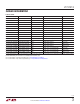
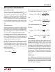
UV Output Voltage vs V
CC
Reset Time-Out Period
vs Capacitance
UV, I
SINK
vs V
CC
TYPICAL PERFORMANCE CHARACTERISTICS
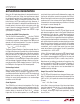
UV/OV, Voltage Output Low
vs Output Sink Current
Reset Timeout Period
vs Temperature
OV/OV Output Voltage vs V
CC
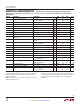
DIS (Pin 8/Pin 1, LTC2912-2): Output Disable Input.
Disables the OV and UV output pins. When DIS is pulled
high, the OV and UV pins are not asserted except during a
UVLO condition. Pin has a weak (2µA) internal pull‑down
to GND. Leave pin open if unused.
Exposed Pad (Pin 9, DDB Package): Exposed Pad may
be left open or connected to device ground.
GND (Pin 5/Pin 4): Device Ground.
LATCH (Pin 8/Pin 1, LTC2912-1, LTC2912-3): OV/OV
Latch Clear/Bypass Input. When pulled high, OV/OV latch
is cleared. While held high, OV/OV has a similar delay and
output characteristic as UV.
OV (Pin 6/Pin 3, LTC2912-1, LTC2912-2): Overvoltage
Logic Output. Asserts low when the VL input voltage is
above threshold. Latched low (LTC2912‑1). Held low for
programmed delay time after VL input is valid (LTC2912‑
2). Pin has a weak pull‑up to V
CC
and may be pulled above
V
CC
using an external pull‑up. Leave pin open if unused.
PIN FUNCTIONS
(DFN/TSOT Packages)
SUPPLY VOLTAGE, V
CC
(V)
0
UV VOLTAGE (V)
3
4
5
4
2912 G07
2
1
0
1
2
3
5
VH = 0.55V
SEL = V
CC
TMR PIN CAPACITANCE, C
TMR
(nF)
10
UV/OV TIMEOUT PERIOD, t
UOTO
(ms)
100
1000
10000
0.1 10 100 1000
2912 G08
1
1
SUPPLY VOLTAGE, V
CC
(V)
0
PULL-DOWN CURRENT, I
UV
(mA)
3
4
5
4
2912 G09
2
1
0
1
2
3
5
VH = 0.45V
SEL = V
CC
UV AT 150mV
UV AT 50mV
0
0
UV/OV, V
OL
(V)
0.2
0.4
0.6
0.8
1.0
5
10 15 20
1912 G10
25
–40°C
30
25°C85°C
I
UV/OV
(mA)
TEMPERATURE (°C)
–50
6
UV/OV TIMEOUT PERIOD, t
OUTO
(ms)
7
8
9
10
12
–25
0 25 50
2912 G11
75 100
11
C
TMR
= 1nF
SUPPLY VOLTAGE, V
CC
(V)
0
OV/OV VOLTAGE (V)
3
OV
OV
4
5
4
2912 G12
2
1
0
1
2
3
5
V
L
= 0.55V