
Datasheet

LTC2928
24
2928f
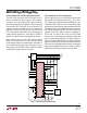
LTC2928 Design Example
The following design example describes a power supply se-
quencing application using many features of the LTC2928.
The example discusses a configuration procedure for the
LTC2928 in a system containing a dual-supply DSP and
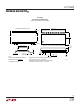
FPGA. The design example schematic is shown in Figure
20. The three main operating phases—sequence-up,
supply monitor, and sequence-down are discussed. All
resistor, capacitor and configuration settings are reviewed.
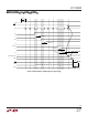
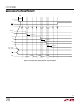
A timing diagram for sequencing-up is shown in Figure
18 and sequencing-down in Figure 19.
A main 3.3V supply provides application power, including
V
CC
for the LTC2928, and is sub-regulated to provide the
lower voltages (2.5V, 1.8V, 1.5V). The LTC2928 controls
external N-channel MOSFETs connected to two of the four
supplies, used to pass power to the loads. The DSP core
is powered from 1.8V and its I/O uses the 3.3V supply.
The FPGA internals are powered from 1.5V and its I/O
uses 2.5V.
1) Configure the LTC2928 based on application
requirements
a. Apply device power.
Since the HV
CC
input is unused, connect it to ground.
Connect the main 3.3V supply to the V
CC
pin. Bypass
V
CC
with 0.1µF to ground.
b. Monitored Supply Polarity
The application monitors four positive voltages. Connect
the voltage selection input (VSEL) to ground (Table 1).
c. Device designations
The application requires only one LTC2928, and it is con-
sidered the MASTER device. By definition, it is also the
FIRST and LAST device. Configure the MASTER/FIRST
designation with the three-state MS1 and MS2 inputs
connected to ground (Table 2). With MS1 and MS2 at
ground, a reset fault is generated if RST pulls low during
the supply monitor phase. Configure LAST device status
with a 3.32k resistor from DONE to V
CC
.
d. Sequence threshold selection
During the sequencing-up or sequencing-down phase,
time positions terminate (CAS is released) when a supply
(or supplies) reaches it sequence threshold. This design
example requires sequence thresholds at 67% of their
under-voltage threshold. Therefore, connect SQT1 to GND
and SQT2 to V
CC
(Table 4).
e. Choose minimum power supply enable spacing
The shortest time between successive power supply
enables (t
CAS(HI)
) is controlled by a capacitor connected
to the STMR pin and ground (also referenced as the se-
quence timer period, t
STMR
). The sequence timer period
for this application is 29ms. Calculate the sequence timer
capacitor from
C
ts
M
STMR F
STMR
()
()
.
=
Ω867
For this application,
C
ms
M
pF
STMR
=
Ω
=
29
867
3300
.
f. Supply order (time position)
The application requires the 1.8V DSP core supply to start
first, about 100ms after the ON signal is received. The 1.8V
supply is monitored on the V3 input and implies selection
of the RT3 resistor, since monitor inputs correspond nu-
merically with the RT and EN inputs. The 100ms required
delay is approximately three sequence timer periods, so
configure the first supply for time position 3 (select RT3
= 24.3k). Table 3 shows the recommended RT resistor
values as a function of time position.
The 3.3V DSP I/O supply (monitored on V4) needs to turn
on just after the core supply is alive, in order to minimize
electrical stress and the possibility of bus contention. Turn
on pass transistor N4 approximately 29ms after the core
supply reaches its sequence threshold by selecting time
position 4 (RT4 = 15k).
The FPGA needs to be powered about 100ms after the
DSP, with its core and I/O supplies enabled simultane-
ously. The 2.5V I/O supply is monitored on V1, and the
1.5V core supply is monitored on V2. Since the required
turn on delay is about three sequence timer periods after
the DSP, select RT1 = RT2 = 3.4k (time position 7).
APPLICATIO S I FOR ATIO
WUU
U