
Datasheet


Table Of Contents
- Features
- Applications
- Description
- Typical Application
- Absolute Maximum Ratings
- Pin Configuration
- Order Information
- Electrical Characteristics
- Typical Performance Characteristics
- Pin Functions
- Block Diagram
- Operation
- Applications Information
- Typical Applications
- Package Description
- Revision History
- Typical Application
- Related Parts
LTC3112
19
3112fc
For more information www.linear.com/LTC3112
applicaTions inForMaTion
Boost Mode Small Signal Model
When stepping up from a lower input voltage to a higher
output voltage, the buck-boost converter will operate in
boost mode where the small signal transfer function from
control voltage, V
COMP
, to the output voltage is given by
the following expression.
V
O
V
COMP
BOOST MODE
= G
BOOST
1+
s
2πf
Z
1–
s
2πf
RHPZ
1+
s
2πf
O
Q
+
s
2πf
O
2
In boost mode operation, the transfer function is character-
ized by a pair of resonant poles and a zero generated by
the
ESR of the output capacitor as in buck mode. However,
in addition there is a right half plane zero which generates
increasing gain and decreasing phase at higher frequen
-
cies. As a result, the crossover frequency in boost mode
operation
generally must be set lower than in buck mode
in order to maintain sufficient phase margin.
The boost mode gain, G
BOOST
, is comprised of two com-
ponents: the pulse width modulator and the power stage.
The gain of the power stage in boost mode is given by the
following equation.
G
POWER
≅
V
OUT
2
1– t
LOW
f
( )
V
IN
By combining the individual terms, the total gain in boost
mode can be reduced to the following expression. Notice
that unlike in buck mode, the gain in boost mode is a
function of both the input and output voltage.
G
BOOST
≅
2•V
OUT
2
V
IN
In boost mode operation, the frequency of the right half
plane zero, f
Z
, is given by the following expression. The
frequency of the right half plane zero decreases at higher
loads and with larger inductors.
f
RHPZ
=
R 1– t
LOW
f
( )
2
V
IN
2
2πL V
OUT
2
In boost mode, the resonant frequency of the power stage
has a dependence on the input and output voltage as shown
by the following equation.
f
O
=
1
2π
R
S
+
RV
IN
2
V
OUT
2
LC
O
R+R
C
( )
≅
1
2π
•
V
IN
V
OUT
1
LC
Finally, the magnitude of the quality factor of the power
stage in boost mode operation is given by the following
expression.
Q =
LC
O
R R
S
+
RV
IN
2
V
OUT
2
L + C
O
R
S
R
Compensation of the Voltage Loop
The small signal models of the LTC3112 reveal that the
transfer function from the error amplifier output, V
COMP
,
to the output voltage is characterized by a set of resonant
poles and a possible zero generated by the ESR of the
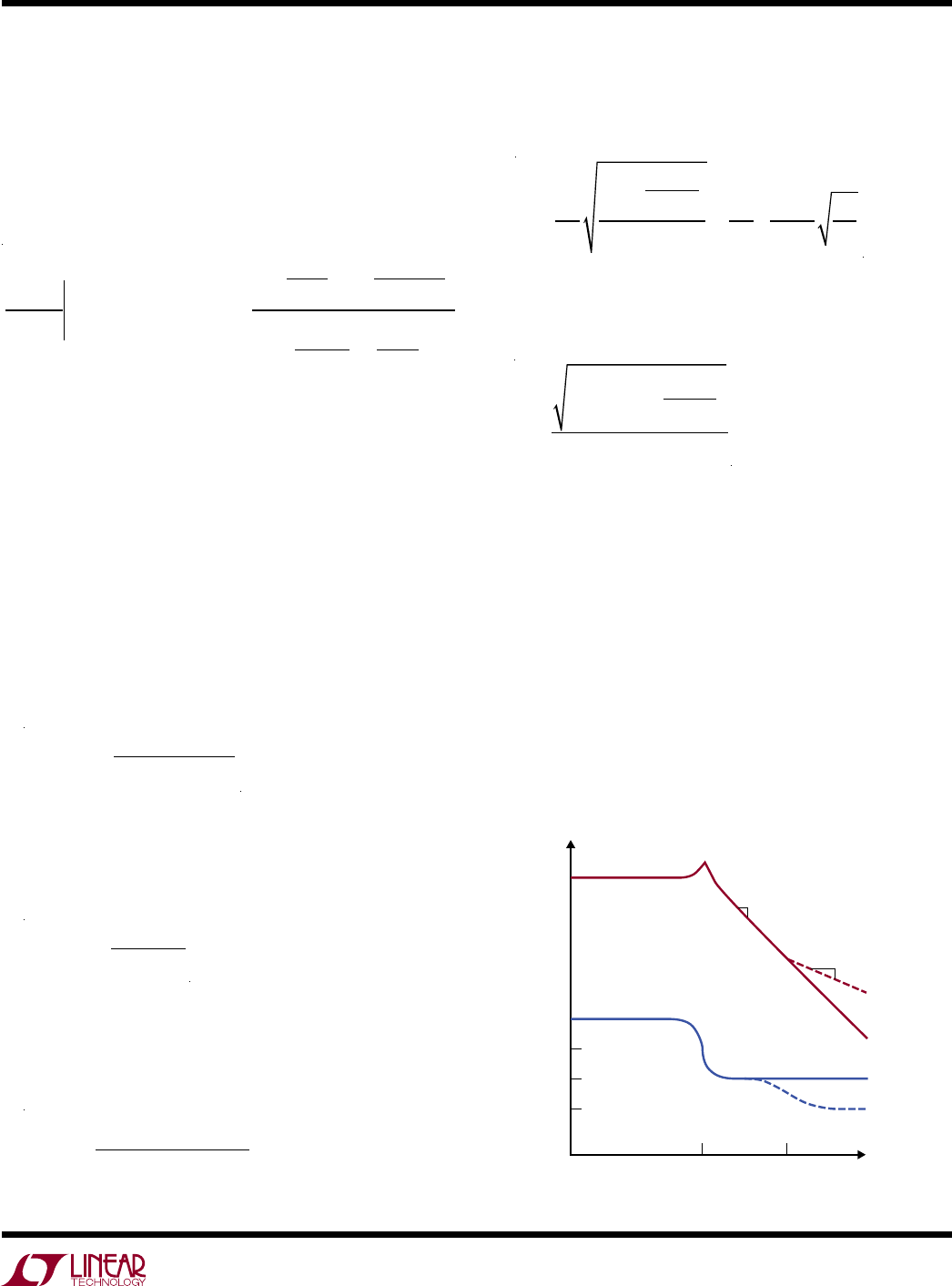
output capacitor as shown in the Bode plot of Figure 4.
In boost mode operation, there is an additional right half
plane zero that produces phase lag and increasing gain at
higher freq uencies. Typically, the compensation network is
designed to ensure that the loop crossover frequency is low
enough that the phase loss from the right half plane zero
is minimized. The low frequency gain in buck mode is a
constant, but varies with both V
IN
and V
OUT
in boost mode.
Figure 4. Buck-Boost Converter Bode Plot
GAIN
PHASE
BOOST MODE
BUCK MODE
–20dB/DEC
–40dB/DEC
f
O
f
3112 F06
f
RHPZ
0°
–90°
–180°
–270°