
Datasheet


LTC3114-1
12
Rev. C
For more information www.analog.com
OPERATION
plifying the PCB layout and design. Factory trimming of
the output current limit offset and gain provide a high
degree of accuracy, typically within ±5% of the setpoint.
The applications section provides details on how to select
the programming resistor, R
PROG
, for the desired average
output current level from the LTC3114-1.
PWM Mode Operation
If the MODE pin is high or if the load current on the
converter is high enough to command PWM mode opera
-
tion with MODE low, the LT
C3114-1 operates in a fixed
1.2MHz PWM mode using a current mode control loop.
PWM mode minimizes output voltage ripple and yields a
low noise switching frequency spectrum. A proprietary
switching algorithm provides seamless transitions be
-
tween operating modes and eliminates discontinuities in
the
average inductor current, inductor ripple current and
loop transfer function throughout all modes of operation.
These advantages result in increased efficiency, improved
loop stability and lower output voltage ripple in comparison
to the traditional buck-boost converter.
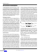
Figure1 shows the topology of the LTC3114-1 power stage
which is comprised of four N-channel DMOS switches and
their associated gate drivers. In PWM mode operation
both switch pins transition on every cycle independent of
the input and output voltages. In response to the internal
control loop command, an internal pulse width modulator
generates the appropriate switch duty cycle to maintain
regulation of the output voltage.
A
PLDO
BST1
C
BST1
C
BST2
L
BST2PV
IN
PV
OUT
SW1 SW2
PLDO
PLDO
PLDO
LTC3114-1
PGND PGND
31141 F01
B
D
C
Figure1. Power Stage Schematic
When stepping down from a high input voltage to a lower
output voltage, the converter operates in buck mode and
switch D remains on for the entire switching cycle except
for the minimum switch low duration (typically 50ns). Dur
-
ing the switch low duration, switch C is turned on which
for
ces SW2 low and charges the flying capacitor, C
BST2
.
This ensures that the switch D gate driver power supply
rail on BST2 is maintained. The duty cycle of switches A
and B are adjusted by the PWM to maintain output voltage
regulation in buck mode.
If the input voltage is lower than the output voltage, the
converter operates in boost mode. Switch A remains on
for the entire switching cycle except for the minimum
switch low duration (typically 100ns). During the switch
low duration, switch B is turned on which forces SW1
low and charges the flying capacitor, C
BST1
. This ensures
that the switch A gate driver power supply rail on BST1
is maintained. The duty cycle of switches C and D are
adjusted by the PWM to maintain output voltage regula
-
tion in boost mode.
Oscillator
The LT
C3114-1 operates from an internal oscillator with
a nominal fixed frequency of 1.2MHz. This allows the
DC/DC converter efficiency to be maximized while still
using small external components.
Downloaded from Arrow.com.Downloaded from Arrow.com.Downloaded from Arrow.com.Downloaded from Arrow.com.Downloaded from Arrow.com.Downloaded from Arrow.com.Downloaded from Arrow.com.Downloaded from Arrow.com.Downloaded from Arrow.com.Downloaded from Arrow.com.Downloaded from Arrow.com.Downloaded from Arrow.com.