
Datasheet


LTC3260
1
3260fa
Typical applicaTion
FeaTures DescripTion
Low Noise Dual Supply
Inverting Charge Pump
The LT C
®
3260 is a low noise dual polarity output power
supply that includes an inverting charge pump with both
positive and negative LDO regulators. The charge pump
operates over a wide 4.5V to 32V input range and can deliver
up to 100mA of output current. Each LDO regulator can
provide up to 50mA of output current. The negative LDO
post regulator is powered from the charge pump output.
The LDO output voltages can be adjusted using external
resistor dividers.
The charge pump employs either low quiescent current
Burst Mode operation or low noise constant frequency
mode. In Burst Mode operation the charge pump V
OUT
regulates to –0.94 • V
IN
, and the LTC3260 draws only
100µA of quiescent current with both LDO regulators on.
In constant frequency mode the charge pump produces
an output equal to –V
IN
and operates at a fixed 500kHz
or to a programmed value between 50kHz to 500kHz us-
ing an external resistor. The LTC3260 is available in low
profile (0.75mm) 3mm x 4mm 14-pin DFN and thermally
enhanced 16-pin MSOP packages.
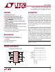
±12V Outputs from a Single 15V Input
LDO Rejection of V
OUT
Ripple
applicaTions
n
V
IN
Range: 4.5V to 32V
n
Inverting Charge Pump Generates –V
IN
n
Charge Pump Output Current Up to 100mA
n
Low Noise Negative LDO Post Regulator
(I
LDO
–
= 50mA Max)
n
Low Noise Independent Positive LDO Regulator
(I
LDO
+
= 50mA Max)
n
100µA Quiescent Current in Burst Mode
®
Operation
with Both LDO Regulators On
n
50kHz to 500kHz Programmable Oscillator Frequency
n
Stable with Ceramic Capacitors
n
Short-Circuit/Thermal Protection
n
Low Profile 3mm × 4mm 14-Pin DFN and Thermally
Enhanced 16-Pin MSOP Packages
n
Low Noise Bipolar/Inverting Supplies
n
Industrial/Instrumentation Low Noise Bias
Generators
n
Portable Medical Equipment
n
Portable Instruments
L, LT , LT C , LT M , Burst Mode, Linear Technology and the Linear logo are registered trademarks
and ThinSOT is a trademark of Linear Technology Corporation. All other trademarks are the
property of their respective owners.
10µF10µF
1µF
10nF
10nF
10µF10µF
909k
909k
200k
100k
100k
12V
–12V
3260 TA01a
LDO
+
15V
LDO
–
ADJ
+
LTC3260
RT
ADJ
–
GND
BYP
+
BYP
–
V
IN
V
OUT
–15V
EN
+
C
–
MODE
EN
–
C
+
V
LDO
+
10mV/DIV
AC-COUPLED
V
LDO
–
10mV/DIV
AC-COUPLED
V
OUT
10mV/DIV
AC-COUPLED
1µs/DIV
3260 TA01b
V
IN
= 15V
V
LDO
+
= 12V
V
LDO
–
= –12V
f
OSC
= 500kHz
I
LDO
+
= 50mA
I
LDO
–
–50mA