
Datasheet


LTC3350
14
3350fc
For more information www.linear.com/LTC3350
operaTion
TiMing DiagraM
Introduction
The LTC3350 is a highly integrated backup power controller
and system monitor. It features a bidirectional switching
controller, input and output ideal diodes, supercapacitor
shunts/balancers, a power-fail comparator, a 14-bit ADC
and I
2
C/SMBus programmability with status reporting.
If V
IN
is above an externally programmable PFI threshold
voltage, the synchronous controller operates in step-down
mode and charges a stack of supercapacitors. A program
-
mable input current limit ensures that the supercapacitors
will automatically be charged at the highest possible charge
current that the input can support. If V
IN
is below the PFI
threshold, then the synchronous controller will run in
reverse as a step-up converter to deliver power from the
supercapacitor stack to V
OUT
.
The two ideal diode controllers drive external MOSFETs to
provide low loss power paths from V
IN
and V
CAP
to V
OUT
.
The ideal diodes work seamlessly with the bidirectional
controller to provide power from the supercapacitors to
V
OUT
without backdriving V
IN
.
The LTC3350 provides balancing and overvoltage protec-
tion to
a series stack of one to four supercapacitors. The
internal
capacitor voltage balancers eliminate the need
for external balance resistors. Overvoltage protection is
provided by
shunt regulators that use an internal switch
and an external resistor across each supercapacitor.
The LTC3350 monitors system voltages, currents, and
die temperature. A general purpose input (GPI) pin is
provided to measure an additional system parameter or
implement a thermistor measurement. In addition, the
LTC3350 can measure the capacitance and resistance of the
supercapacitor stack. This provides indication of the health
of the supercapacitors and, along with the V
CAP
voltage
measurement, provides information on the total energy
stored and the maximum power that can be delivered.
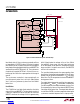
Bidirectional Switching Controller—Step-Down Mode
The bidirectional switching controller is designed to charge
a series stack of supercapacitors (Figure 1). Charging
proceeds at a constant current until the supercapacitors
reach their maximum charge voltage determined by the
CAPFB servo voltage and the resistor divider between V
CAP
and CAPFB. The maximum charge current is determined
by the value of the sense resistor, R
SNSC
, used in series
with the inductor. The charge current loop servos the
voltage across the sense resistor to 32mV. When charging
begins, an internal soft-start ramp will increase the charge
current from zero to full current in 2ms. The V
CAP
voltage
and charge current can be read from the meas_vcap and
meas_ichrg registers, respectively.
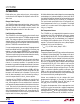
SDA
SCL
S Sr P S
t
HD(SDA)
S = START, Sr = REPEATED START, P = STOP
t
HD(DAT)
t
SU(STA)
t
SU(STO)
t
SU(DAT)
t
LOW
t
HD(SDA)
t
SP
t
BUF
t
r
t
f
t
r
t
f
t
HIGH
3350 TD
Definition of Timing for F/S Mode Devices on the I
2
C Bus
Downloaded from Arrow.com.Downloaded from Arrow.com.Downloaded from Arrow.com.Downloaded from Arrow.com.Downloaded from Arrow.com.Downloaded from Arrow.com.Downloaded from Arrow.com.Downloaded from Arrow.com.Downloaded from Arrow.com.Downloaded from Arrow.com.Downloaded from Arrow.com.Downloaded from Arrow.com.Downloaded from Arrow.com.Downloaded from Arrow.com.