
Datasheet


LTC3406AB
3
3406abfa
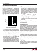
INPUT VOLTAGE (V)
2
EFFICIENCY (%)
6
3406B G01
3
4
5
100
90
80
70
60
50
40
30
20
10
0
I
L
= 100mA
I
L
= 600mA
I
L
= 10mA
V
OUT
= 1.8V
ELECTRICAL CHARACTERISTICS
Note 1: Stresses beyond those listed under Absolute Maximum Ratings
may cause permanent damage to the device. Exposure to any Absolute
Maximum Rating condition for extended periods may affect device
reliability and lifetime.
Note 2: The LTC3406ABE is guaranteed to meet performance
specifi cations from 0°C to 85°C. Specifi cations over the –40°C to 85°C
operating temperature range are assured by design, characterization and
correlation with statistical process controls.
Note 3: T
J
is calculated from the ambient temperature T
A
and power
dissipation P
D
according to the following formula:
LTC3406AB: T
J
= T
A
+ (P
D
)(250°C/W)
The ● denotes the specifi cations which apply over the full operating
temperature range, otherwise specifi cations are at T
A
= 25°C. V
IN
= 3.6V unless otherwise specifi ed.
SYMBOL PARAMETER CONDITIONS MIN TYP MAX UNITS
V
RUN
RUN Threshold
●
0.3 1 1.5 V
I
RUN
RUN Leakage Current
●
±0.01 ±1 μA
Note 4: The LTC3406AB is tested in a proprietary test mode that connects
V
FB
to the output of the error amplifi er.
Note 5: Dynamic supply current is higher due to the gate charge being
delivered at the switching frequency.
Note 6: This IC includes overtemperature protection that is intended
to protect the device during momentary overload conditions. Junction
temperature will exceed 125°C when overtemperature protection is active.
Continuous operation above the specifi ed maximum operating junction
temperature may impair device reliability.
Note7: Limited by long term current density considerations.
Effi ciency vs Input Voltage Effi ciency vs Load Current
Effi ciency vs Load Current
Reference Voltage vs
Temperature
TYPICAL PERFORMANCE CHARACTERISTICS
(From Front Page Figure Except for the Resistive Divider Resistor Values)
OUTPUT CURRENT (mA)
0.1
EFFICIENCY (%)
10
1000
100
90
80
70
60
50
40
30
20
10
0
3406B G02
1 100
V
OUT
= 1.2V
V
IN
= 2.7V
V
IN
= 3.6V
V
IN
= 4.2V
OUTPUT CURRENT (mA)
0.1
EFFICIENCY (%)
10
1000
100
90
80
70
60
50
40
30
20
10
0
3406B G03
1 100
V
OUT
= 2.5V
V
IN
= 2.7V
V
IN
= 3.6V
V
IN
= 4.2V
TEMPERATURE (°C)
–50
REFERENCE VOLTAGE (V)
0.605
0.610
0.615
25 75
3406AB G21
0.600
0.595
–25 0
50 100 125
0.590
0.585
V
IN
= 3.6V