
Datasheet


LTC3407
12
3407fa
APPLICATIONS INFORMATION
the regulator operating in a 70°C ambient temperature is
approximately:
T
J
= 2 • 0.153 • 45 + 70 = 84°C
which is below the absolute maximum junction tempera-
ture of 125°C.
Design Example
As a design example, consider using the LTC3407 in an
portable application with a Li-Ion battery. The battery pro-
vides a V
IN
= 2.8V to 4.2V. The load requires a maximum
of 600mA in active mode and 2mA in standby mode. The
output voltage is V
OUT
= 2.5V. Since the load still needs
power in standby, Burst Mode operation is selected for
good low load effi ciency.
First, calculate the inductor value for about 30% ripple
current at maximum V
IN
:
L ≥
2.5V
1.5MHz • 300mA
•1–
2.5V
4.2V
⎛
⎝
⎜
⎞
⎠
⎟
= 2.25μH
Choosing the closest inductor from a vendor of 2.2μH
inductor, results in a maximum ripple current of:
ΔI
L
=
2.5V
1.5MHz • 2.2μH
•1−
2.5V
4.2V
⎛
⎝
⎜
⎞
⎠
⎟
= 307mA
For cost reasons, a ceramic capacitor will be used. C
OUT
selection is then based on load step droop instead of ESR
requirements. For a 5% output droop:
C
OUT
≈ 3
600mA
1.5MHz •(5% • 2.5V)
= 9.6μF
The closest standard value is 10μF. Since the output imped-
ance of a Li-Ion battery is very low, C
IN
is typically 10μF.
The output voltage can now be programmed by choosing
the values of R1 and R2. To maintain high effi ciency, the
current in these resistors should be kept small. Choosing
2μA with the 0.6V feedback voltage makes R1~300k. A close
standard 1% resistor is 280k, and R2 is then 887k.
The POR pin is a common drain output and requires a pull-
up resistor. A 100k resistor is used for adequate speed.
Figure 1 shows the complete schematic for this design
example.
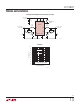
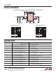
Board Layout Considerations
When laying out the printed circuit board, the following
checklist should be used to ensure proper operation of
the LTC3407. These items are also illustrated graphically
in the layout diagram of Figure 3. Check the following in
your layout:
1. Does the capacitor C
IN
connect to the power V
IN
(Pin
3) and GND (exposed pad) as close as possible? This
capacitor provides the AC current to the internal power
MOSFETs and their drivers.
2. Are the C
OUT
and L1 closely connected? The (–) plate of
C
OUT
returns current to GND and the (–) plate of C
IN
.
3. The resistor divider, R1 and R2, must be connected
between the (+) plate of C
OUT
and a ground sense line
terminated near GND (Exposed Pad). The feedback signals
V
FB
should be routed away from noisy components and
traces, such as the SW line (Pins 4 and 7), and its trace
should be minimized.
4. Keep sensitive components away from the SW pins. The
input capacitor C
IN
and the resistors R1 to R4 should be
routed away from the SW traces and the inductors.
5. A ground plane is preferred, but if not available, keep
the signal and power grounds segregated with small signal
components returning to the GND pin at one point and
should not share the high current path of C
IN
or C
OUT
.
6. Flood all unused areas on all layers with copper. Flood-
ing with copper will reduce the temperature rise of power
components. These copper areas should be connected to
V
IN
or GND.
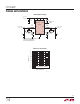
Figure 3. LTC3407 Layout Diagram (See Board Layout Checklist)
RUN2 V
IN
V
IN
V
OUT2
V
OUT1
RUN1
POR
SW1
V
FB1
GND
V
FB2
SW2
MODE/SYNC
LTC3407
C
IN
C4C5
L1
L2
R4 R2
R1
R3
C
OUT2
C
OUT1
3407 F03
BOLD LINES INDICATE HIGH CURRENT PATHS