
Datasheet


LTC3414
12
3414fb
Design Example
As a design example, consider using the LTC3414 in an
application with the following specifications:
V
IN
= 2.7V to 4.2V, V
OUT
= 2.5V, I
OUT(MAX)
= 4A,
I
OUT(MIN)
= 100mA, f = 1MHz.
Because efficiency is important at both high and low load
current, Burst Mode operation will be utilized.
First, calculate the timing resistor:
Rkk
OSC
==
308 10
110
10 298
11
6
.•
•
–
Use a standard value of 294k. Next, calculate the inductor
value for about 40% ripple current at maximum V
IN
:
L
V
MHz A
V
V
H=
⎛
⎝
⎜
⎞
⎠
⎟
⎛
⎝
⎜
⎞
⎠
⎟
= μ
25
116
1
25
42
063
.
()(.)
–
.
.
.
Using a 0.47μH inductor results in a maximum ripple
current of:
Δ =
μ
⎛
⎝
⎜
⎞
⎠
⎟
⎛
⎝
⎜
⎞
⎠
⎟
=I
V
MHz H
V
V
A
L
25
1047
1
25
42
215
.
()(. )
–
.
.
.
C
OUT
will be selected based on the ESR that is required to
satisfy the output voltage ripple requirement and the bulk
capacitance needed for loop stability. For this design, a
22μF ceramic capacitor and a 470μF tantalum capacitor
will be used.
C
IN
should be sized for a maximum current rating of:
IA
V
V
V
V
A
RMS RMS
=
⎛
⎝
⎜
⎞
⎠
⎟
=()
.
.
.
.
–.4
25
42
42
25
1196
Decoupling the PV
IN
and SV
IN
pins with two 22μF capaci-
tors and a 330μF tantalum capacitor is adequate for most
applications.
The burst clamp and output voltage can now be pro-
grammed by choosing the values of R1, R2, and R3. The
voltage on pin MODE will be set to 0.49V by the resistor
divider consisting of R2 and R3. A burst clamp voltage of
0.49V will set the minimum inductor current, I
BURST
, as
follows:
IV V
A
V
A
BURST BURST
=
()
⎛
⎝
⎜
⎞
⎠
⎟
=–.
.
.
.0 383
69
06
123
If we set the sum of R2 and R3 to 200k, then the following
equations can be solved:
RR k
R
R
V
V
2 3 200
1
2
3
08
049
+=
+=
.
.
The two equations shown above result in the following
values for R2 and R3: R2 = 78.7k , R3 = 124k. The value
of R1 can now be determined by solving the following
equation.
1
1
202 7
25
08
1 432
+=
=
R
k
V
V
Rk
.
.
.
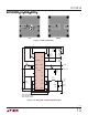
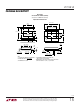
A value of 432k will be selected for R1. Figure 4 shows the
complete schematic for this design example.
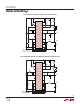
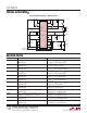
PC Board Layout Checklist
When laying out the printed circuit board, the following
checklist should be used to ensure proper operation of the
LTC3414. Check the following in your layout:
1. A ground plane is recommended. If a ground plane layer
is not used, the signal and power grounds should be
segregated with all small signal components returning to
the SGND pin at one point which is then connected to the
PGND pin close to the LTC3414.
2. Connect the (+) terminal of the input capacitor(s), C
IN
,
as close as possible to the PV
IN
pin. This capacitor
provides the AC current into the internal power MOSFETs.
3. Keep the switching node, SW, away from all sensitive
small signal nodes.
4. Flood all unused areas on all layers with copper.
Flooding with copper will reduce the temperature rise of
power components. You can connect the copper areas to
any DC net (PV
IN
, SV
IN
, V
OUT
, PGND, SGND, or any other
DC rail in your system).
5. Connect the V
FB
pin directly to the feedback resistors.
The resistor divider must be connected between V
OUT
and SGND.
APPLICATIO S I FOR ATIO
WUUU