
Datasheet


LTC3417A-2
7
3417a2fa
–
+
–
+
–
+
–
+
–
+
I
TH
LIMIT
I
TH1
1.5A REGULATOR
1A REGULATOR
V
B
0.752V
0.752V
V
B
0.848V
0.848V
V
IN1
SW1
PGND1
PHASE
SLOPE
COMPENSATION
ANTI-SHOOT-
THROUGH
OSCILLATOR
LOGIC
–
+
–
+
V
FB1
–
+
–
+
–
+
–
+
–
+
–
+
–
+
SYNC/MODE
I
TH2
V
IN2
3417A-2 BD
FREQ
PGND2
SW2
SLOPE
COMPENSATION
ANTI-SHOOT-
THROUGH
I
TH
LIMIT
LOGIC
VOLTAGE
REFERENCE
RUN1
RUN2
PGOOD
V
FB2
V
IN2
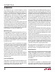
FUNCTIONAL DIAGRAM
PIN FUNCTIONS
V
IN
, the 1.5A regulator and the 1A regulator are in phase.
When PHASE is at 0V, the 1.5A regulator and the 1A
regulator are switching 180 degrees out-of-phase. Do
not fl oat this pin.
SW1 ( Pi n 15/ Pi n 18) : Switch Node Connection to the
Inductor for the 1.5A Regulator. This pin swings from
V
IN1
to PGND1.
PGND1 ( Pi n 16/ Pi n 19) : Ground for SW1 N-Channel Driver.
PGND2 , GNDD ( Pi ns 1, 10 , 11 , 20 ) : TSSOP Package Only.
Ground for SW2 N-channel driver and digital ground for
circuit.
Exposed Pad ( Pi n 17/ Pi n 21) : PGND2, GNDD. Ground for
SW2 N-channel driver and digital ground for circuit. The
Exposed Pad must be soldered to PCB ground.
( DFN/ TSSOP)