
Datasheet


11
LTC3445
3445fa
TI I G DIAGRA
UWW
t
BUF
t
SUSTO
3445 TD
t
HD(STA)
t
HD(DAT)
t
SU(STA)
t
SU(DAT)
t
LOW
t
HIGH
t
r
t
f
t
HD(STA)
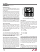
SCL
SDA
START
CONDITION
REPEATED START
CONDITION
STOP
CONDITION
START
CONDITION
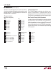
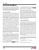
I
2
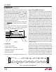
C Fast Mode Timing Specifications (for Reference)
SYMBOL PARAMETER MIN TYP MAX UNITS
f
I2C(MAX)
Maximum I
2
C Operating Frequency 0 400 kHz
t
BUF
Bus Free Time Between Stop and Start Condition 1.3 µs
t
HD(RSTA)
Hold Time After (Repeated) Start Condition 0.6 µs
t
SU(RSTA)
Repeated Start Condition Setup Time 0.6 µs
t
SU(STOP)
Stop Condition Setup Time 0.6 µs
t
HD(DAT)
Data Hold Time 0 0.9 ns
t
SU(DAT)
Data Setup Time 100 ns
t
LOW
Clock Low Period 1.3 µs
t
HIGH
Clock High Period 0.6 µs
t
SP
Pulse Width of Spikes Suppressed by Input Filter 0 50 ns
t
f
Clock, Data Fall Time (Note 1) 20 + 0.1 300 ns
• C
B
tr Clock, Data Rise Time (Note 1) 20 + 0.1 300 ns
• C
B
Note 1: C
B
= Capacitance of one bus line.
OPERATIO
U
(refer to Figure 1)
BUCK REGULATOR
Main Control Loop
The LTC3445 uses a constant or spread spectrum fre-
quency, current mode step-down architecture (Figure 2).
Both the main (P-channel MOSFET) and synchronous
(N-channel MOSFET) switches are internal. During normal
operation, the internal top power MOSFET is turned on
each cycle when the oscillator sets the RS latch, and
turned off when the current comparator, I
COMP
, resets the
RS latch. The peak inductor current at which I
COMP
resets
the RS latch is controlled by the output of error amplifier
EA. When the load current increases, it causes a slight
decrease in the feedback voltage, FB, relative to an internal
reference voltage, which in turn, causes the EA’s output
voltage to increase until the average inductor current
matches the new load current. While the top MOSFET is
off, the bottom MOSFET is turned on until either the
inductor current starts to reverse, as indicated by the
current reversal comparator I
RCMP
, or the beginning of the
next clock cycle.