
Datasheet


16
LTC3445
3445fa
1
2
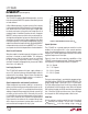
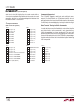
C Register Definitions
(POR = 00 for all registers)
REG 0 REG 1
7 0 (Logic Low) 7 0 (Logic Low)
6 0 (Logic Low) 6 0 (Logic Low)
5 Buck DAC5 5 0 (Logic Low)
4 Buck DAC4 4 0 (Logic Low)
3 Buck DAC3 3 0 (Logic Low)
2 Buck DAC2 2 0 (Logic Low)
1 Buck DAC1 1 Slew Rate 1
0 Buck DAC0 0 Slew Rate 0
REG 2 REG 3
7 0 (Logic Low) 7 PGOOD Blank Disable
6 0 (Logic Low) 6 0 (Logic Low)
5 0 (Logic Low) 5 0 (Logic Low)
4 STATUS—Buck Thermal Shutdown 4 0 (Logic Low)
3 STATUS—Buck PGOODb 3 BURST Mode
2 STATUS—LDO2 PGOODb 2 LDO2 Disable
1 STATUS—LDO1 PGOODb 1 LDO1 Disable
0 Buck Update (GO Bit) 0 Buck Disable
OPERATIO
U
(refer to Figure 1)
REG 5
7 0 (Logic Low)
6 % SPR1
5 % SPR0
4 (Logic Low)
3 (Logic Low)
2 (Logic Low)
1 (Logic Low)
0 (Logic Low)
data line is also left high by the slave and master after a
slave has transmitted a byte of data to the master in a read
operation, but this is a not-acknowledge that indicates that
the data transfer is successful.
Commands Supported
The LTC3445 supports read byte and write byte com-
mands. For the ACK bits, an S indicates that the slave is
pulling the data line low and an M indicates that the master
is effectively acknowledging by leaving the data line high.
Data Transfer Timing for Write Commands
In order to help assure that bad data is not written into the
part, data from a write command is only stored after a
valid acknowledge has been performed. The part will
detect that SDA is low on the rising edge of SCL that marks
the end of the period in which the LTC3445 acknowledges
the data write and then latch the data during the following
SCL low period.