
Datasheet


LTC3530
6
3530fb
–
+
–
+
–
+
–
+
–
+
7
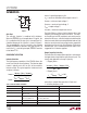
PWM
LOGIC
GATE
DRIVERS
AND
ANTICROSS
CONDUCTION
GND
OSC
SW A
SW1
V
IN
SW2
SW D
ANTI-RING
ERROR
AMP
1.215V
REVERSE
AMP
SW B SW C
5
3 4
V
OUT
6
FB
9
BURST
2
V
C
10
8
SHDN/SS
1
R
T
3530 BD
PWM
COMPARATORS
THERMAL
SHUTDOWN
SHUTDOWN
SOFT-START
SHUTDOWN
1.215V
V
REF
AUTOMATIC
BURST MODE
CONTROL
G
m
= 1/60k
2A
V
REF
SLEEP
L1
C
IN
C
OUT
C
BURST
C
P1
R
SS
C
SS
R
T
R2
R1
R
BURST
GND (Pin 5): Ground for the IC.
V
OUT
(Pin 6): Output of the Synchronous Rectifi er. A fi lter
capacitor is placed from V
OUT
to GND. A ceramic bypass
capacitor is recommended as close to the V
OUT
and GND
pins as possible.
V
IN
(Pin 7): Input Supply Voltage. Internal V
CC
for the IC.
A 10μF ceramic capacitor is recommended as close to the
V
IN
and GND pins as possible.
SHDN/SS (Pin 8): Combined Soft-Start and Shutdown.
Applied voltage <0.4V shuts down the IC. Tie to >1.4V to
enable the IC and >1.6V to ensure the error amp is not
clamped from soft-start. An R-C from the shutdown com-
mand signal to this pin will provide a soft-start function
by limiting the rise time of V
C
.
FB (Pin 9): Feedback Pin. Connect resistor divider tap here.
The output voltage can be adjusted from 1.8V to 5.25V.
The feedback reference is typically 1.215V.
V
OUT
= 1.215V • 1+
R1
R2
V
C
(Pin10): Error Amp Output. An R-C network is con-
nected from this pin to FB for loop compensation. Refer
to “Closing the Feedback Loop” section for component
selection guidelines. During Burst Mode operation, V
C
is
internally clamped.
Exposed Pad (Pin 11, DD Package Only): Ground. This
pin must be soldered to the PCB and electrically connected
to ground.
PIN FUNCTIONS
BLOCK DIAGRAM