
Datasheet

LTC3561A
17
3561af
APPLICATIONS INFORMATION
The closest standard value is 22μF. Since the output
impedance of a Li-Ion battery is very low, C
IN
is typically
10μF. In noisy environments, decoupling SV
IN
from PV
IN
with an R6/C8 fi lter of 1Ω/0.1μF may help, but is typically
not needed.
For the feedback resistors, choose R1 = 200k, R2 can be
calculated from:
R
V
R
V
V
k
OUT
2
08
11
18
08
1 200=
⎛
⎝
⎜
⎞
⎠
⎟
=
⎛
⎝
⎜
⎞
⎠
⎟
.
–•
.
.
–• == 250k
Choose a standard value of 249k for R2.
The compensation should be optimized for these compo-
nents by examining the load step response but a good place
to start for the LTC3561A is with a 16.9kΩ and 680pF fi lter.
The output capacitor may need to be increased depending
on the actual undershoot during a load step.
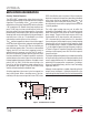
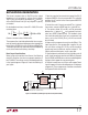
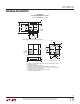
Board Layout Considerations
When laying out the printed circuit board, the following
checklist should be used to ensure proper operation of
the LTC3561A. These items are also illustrated graphically
in the layout diagram of Figure 6. Check the following in
your layout:
1. Does the capacitor C
IN
connect to the power V
IN
(Pin 5)
and power GND (Pin 4) as close as possible? This capacitor
provides the AC current to the internal power MOSFETs
and their drivers.
2. Are the C
OUT
and L1 closely connected? The (–) plate of
C
OUT
returns current to PGND and the (–) plate of C
IN
.
3. The resistor divider, R1 and R2, must be connected
between the (+) plate of C
OUT
and a ground line termi-
nated near SGND (Exposed Pad). The feedback signal
V
FB
should be routed away from noisy components and
traces, such as the SW line (Pin 3), and its trace should
be minimized.
4. Keep sensitive components away from the SW pin. The
input capacitor C
IN
, the compensation capacitor C
C
and
C
ITH
and all the resistors R1, R2, R
T
, and R
C
should be
routed away from the SW trace and the inductor L1. The
SW pin pad should be kept as small as possible.
5. A ground plane is preferred, but if not available, route all
small-signal components back to the SGND pin (Exposed
Pad). All SGND and PGND pins must be connected together
through a thick copper trace or ground plane.
6. Flood all unused areas on all layers with copper. Flood-
ing with copper will reduce the temperature rise of power
components. These copper areas should be connected to
the Exposed Pad for best results.
Figure 6. LTC3561A Layout Diagram (See Board Layout Checklist)
PV
IN
LTC3561A
PGND
SW
SV
IN
SGNDV
FB
I
TH
SHDN/R
T
L1
V
IN
V
OUT
R
T
R
C
R1R2
3561A F06
C
C
C
ITH
BOLD LINES INDICATE HIGH CURRENT PATHS
C
IN
C
OUT
C4