LTC3577/LTC3577-1 Highly Integrated 6-Channel Portable PMIC DESCRIPTION FEATURES n n n n n n n n n n n n n Full Featured Li-Ion/Polymer Charger/PowerPath™ Controller with Instant-On Operation Triple Adjustable High Efficiency Step-Down Switching Regulators (800mA, 500mA, 500mA IOUT) 6μA Battery Drain Current in Hard Reset Bat-Track™ Control for External HV Buck DC/DCs I2C Adjustable SW Slew Rates for EMI Reduction High Temperature Battery Voltage Reduction Improves Safety and Reliability Overvoltage Protec
LTC3577/LTC3577-1 TABLE OF CONTENTS Features ............................................................................................................................ 1 Applications ....................................................................................................................... 1 Typical Application ............................................................................................................... 1 Description............................................................
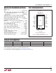
LTC3577/LTC3577-1 ABSOLUTE MAXIMUM RATINGS PIN CONFIGURATION (Notes 1, 2, 3) 44 CHRG 43 CLPROG 42 VC 41 ACPR 40 VBUS 39 VOUT 38 BAT TOP VIEW ILIM0 1 ILIM1 2 LED_FS 3 WALL 4 SW3 5 VIN3 6 FB3 7 OVSENS 8 LED_OV 9 DVCC 10 SDA 11 SCL 12 OVGATE 13 PWR_ON 14 ON 15 45 GND 37 IDGATE 36 PROG 35 NTC 34 NTCBIAS 33 SW1 32 VIN12 31 SW2 30 VINLD02 29 LDO2 28 LDO1 27 LDO1_FB 26 FB1 25 FB2 24 LDO2_FB 23 VINLDO1 PBSTAT 16 WAKE 17 SW 18 SW 19 SW 20 PG_DCDC 21 ILED 22 VSW ...............................................
LTC3577/LTC3577-1 ELECTRICAL CHARACTERISTICS Power Manager. The l denotes the specifications which apply over the full operating temperature range, otherwise specifications are at TA = 25°C. VBUS = 5V, VBAT = 3.8V, ILIM0 = ILIM1 = WALL = 0V, VINLDO1 = VINLDO2 = VIN12 = VIN3 = VOUT, RPROG = 2k, RCLPROG = 2.1k, unless otherwise noted. SYMBOL PARAMETER CONDITIONS MIN TYP MAX UNITS 90 475 950 100 500 1000 mA mA mA 0.42 0.042 0.
LTC3577/LTC3577-1 ELECTRICAL CHARACTERISTICS Power Manager. The l denotes the specifications which apply over the full operating temperature range, otherwise specifications are at TA = 25°C. VBUS = 5V, VBAT = 3.8V, ILIM0 = ILIM1 = WALL = 0V, VINLDO1 = VINLDO2 = VIN12 = VIN3 = VOUT, RPROG = 2k, RCLPROG = 2.1k, unless otherwise noted. SYMBOL PARAMETER CONDITIONS MIN TYP MAX UNITS NTC, Battery Discharge Protection VCOLD Cold Temperature Fault Threshold Voltage Rising NTC Voltage Hysteresis 75 76 1.
LTC3577/LTC3577-1 ELECTRICAL CHARACTERISTICS I2C Interface. The l denotes the specifications which apply over the full operating temperature range, otherwise specifications are at TA = 25°C. DVCC = 3.3V, VOUT = 3.8V, unless otherwise noted. SYMBOL PARAMETER DVCC Input Supply Voltage IDVCC DVCC Supply Current VDVCC,UVLO DVCC UVLO CONDITIONS MIN TYP 1.6 SCL = 400kHz SCL = SDA = 0kHz MAX UNITS 5.5 V 1 0.4 μA μA 1.
LTC3577/LTC3577-1 ELECTRICAL CHARACTERISTICS Step-Down Switching Regulators. The l denotes the specifications which apply over the full operating temperature range, otherwise specifications are at TA = 25°C. VOUT = VIN12 = VIN3 = 3.8V, all regulators enabled unless otherwise noted.
LTC3577/LTC3577-1 ELECTRICAL CHARACTERISTICS LDO Regulators. The l denotes the specifications which apply over the full operating temperature range, otherwise specifications are at TA = 25°C. VINLDO1 = VINLDO2 = VOUT = VBAT = 3.8V, LDO1 and LDO2 enabled unless otherwise noted. SYMBOL PARAMETER CONDITIONS MIN TYP ILDO1_SC Short-Circuit Output Current VDROP1 Dropout Voltage (Note 12) ILDO1 = 150mA, VINLDO1 = 3.6V ILDO1 = 150mA, VINLDO1 = 2.5V ILDO1 = 75mA, VINLDO1 = 1.
LTC3577/LTC3577-1 ELECTRICAL CHARACTERISTICS Pushbutton Controller. The l denotes the specifications which apply over the full operating temperature range, otherwise specifications are at TA = 25°C. VOUT = 3.8V, unless otherwise noted.
LTC3577/LTC3577-1 ELECTRICAL CHARACTERISTICS Note 1: Stresses beyond those listed under Absolute Maximum Ratings may cause permanent damage to the device. Exposure to any Absolute Maximum Rating condition for extended periods may affect device reliability and lifetime. Note 2: The LTC3577E/LTC3577E-1 are guaranteed to meet performance specifications from 0°C to 85°C.
LTC3577/LTC3577-1 TYPICAL PERFORMANCE CHARACTERISTICS TA = 25°C unless otherwise specified Input Current Limit vs Temperature 1000 300 VBUS = 5V RCLPROG = 2.1k 10x MODE 500 260 900 800 240 700 220 600 RON (mΩ) IVBUS (mA) 600 IOUT = 400mA 280 5x MODE 500 VBUS = 4.5V 180 VBUS = 5.5V 160 400 120 200 1x MODE 100 0 –50 –25 50 25 0 75 TEMPERATURE (°C) 100 0 –50 125 –25 50 25 0 75 TEMPERATURE (°C) 6 5 200 SAFETY TIMER 2 TERMINATION RCLPROG = 2.
LTC3577/LTC3577-1 TYPICAL PERFORMANCE CHARACTERISTICS TA = 25°C unless otherwise specified Input Connect Waveform Input Disconnect Waveform Switching from 1x to 5x Mode VBUS 5V/DIV VBUS 5V/DIV VOUT 5V/DIV VOUT 5V/DIV IBUS 0.5A/DIV IBUS 0.5A/DIV IBUS 0.5A/DIV IBAT 0.5A/DIV IBAT 0.5A/DIV IBAT 0.5A/DIV VBAT = 3.75V IOUT = 100mA RCLPROG = 2k RPROG = 2k 1ms/DIV 3577 G13 ILIM0/ILIM1 5V/DIV VBAT = 3.
LTC3577/LTC3577-1 TYPICAL PERFORMANCE CHARACTERISTICS TA = 25°C unless otherwise specified 100 100 90 90 Burst Mode OPERATION EFFICIENCY (%) 70 60 PULSE-SKIPPING MODE 50 1500 Burst Mode OPERATION 1400 80 40 70 EFFICIENCY (%) 80 PULSE-SKIPPING MODE 60 50 40 30 30 20 0 0.01 20 VOUT3 = 1.2V VIN3 = 3.8V VIN3 = 5V 10 0.1 1 10 IOUT (mA) 100 VOUT3 = 2.5V VIN3 = 3.8V VIN3 = 5V 10 0 0.01 1000 0.1 1 10 IOUT (mA) 100 1100 1000 900 500mA BUCK 800 700 VINx = 3.
LTC3577/LTC3577-1 TYPICAL PERFORMANCE CHARACTERISTICS TA = 25°C unless otherwise specified OVP Connection Waveform OVP Protection Waveform OVP Reconnection Waveform VBUS 5V/DIV VBUS 5V/DIV VBUS 5V/DIV OVGATE 5V/DIV OVGATE 5V/DIV OVP INPUT VOLTAGE 5V TO 10V STEP 5V/DIV OVP INPUT VOLTAGE 0V TO 5V STEP 5V/DIV 3577 G31 500μs/DIV Rising Overvoltage Threshold vs Temperature OVSENS Quiescent Current vs Temperature OVSENS CONNECTED TO INPUT THROUGH 10 6.2k RESISTOR 31 8 OVGATE (V) 33 6.270 6.
LTC3577/LTC3577-1 TYPICAL PERFORMANCE CHARACTERISTICS TA = 25°C unless otherwise specified LED Driver Efficiency 6 LEDs LED Boost Current Limit vs Temperature LED Driver Efficiency 4 LEDs 90 90 85 85 80 80 1200 1100 75 70 65 3V 3.6V 4.2V 4.8V 5.5V 60 55 50 0 2 4 6 75 70 65 3V 3.6V 4.2V 4.8V 5.
LTC3577/LTC3577-1 PIN FUNCTIONS ILIM0, ILIM1 (Pins 1, 2): Input Current Control Pins. ILIM0 and ILIM1 control the input current limit. See Table 1 in the “USB PowerPath Controller” section. Both pins are pulled low by a weak current sink. LED_FS (Pin 3): A resistor between this pin and ground sets the full-scale output current of the ILED pin. WALL (Pin 4): Wall Adapter Present Input. Pulling this pin above 4.3V will disconnect the power path from VBUS to VOUT .
LTC3577/LTC3577-1 PIN FUNCTIONS ILED (Pin 22): Series LED Backlight Current Sink Output. This pin is connected to the cathode end of the series LED backlight string. The current drawn through the series LEDs can be programmed via a 6-bit 60dB DAC and dimmed via an internal 4-bit PWM function. I2C is used to control LED driver enable, brightness, gradation (soft on/soft off). I2C default is LED driver off, current = 0mA. VINLDO1 (Pin 23): Input Supply of Low Dropout Linear Regulator 1 (LDO1).
LTC3577/LTC3577-1 PIN FUNCTIONS VBUS (Pin 40): USB Input Voltage. VBUS will usually be connected to the USB port of a computer or a DC output wall adapter. VBUS should be bypassed with a low impedance multilayer ceramic capacitor. ACPR (Pin 41): Wall Adapter Present Output (Active Low). A low on this pin indicates that the wall adapter input comparator has had its input pulled above its input threshold (typically 4.3V).
LTC3577/LTC3577-1 BLOCK DIAGRAM 8 13 OVSENS 4 OVERVOLTAGE PROTECTON 40 43 34 35 1 2 44 41 WALL OVGATE 42 ACPR VC WALL DETECT VC CONTROL VOUT VBUS INPUT CURRENT LIMIT CLPROG NTCBIAS NTC BATTERY TEMP MONITOR IDEAL DIODE – + OVERTEMP BATTERY SAFETY DISCHARGE ILIM LOGIC EN 500mA, 2.25MHz BUCK REGULATOR 15 16 10 11 12 BAT VIN12 SW1 CHRG 0.
LTC3577/LTC3577-1 OPERATION PowerPath OPERATION Introduction The LTC3577 is a highly integrated power management IC that features: – PowerPath controller – Battery charger – Ideal diode – Input overvoltage protection – Pushbutton controller – Three step-down switching regulators – High voltage buck regulator VC controller – Two low dropout linear regulators – 40V LED backlight controller Designed specifically for USB applications, the PowerPath controller incorporates a precision input current limit which co
LTC3577/LTC3577-1 OPERATION a small voltage above the BAT pin voltage. This control method provides a high input voltage, high efficiency battery charger and PowerPath function. The LTC3577 also includes a pushbutton input to control the three synchronous step-down switching regulators and system reset. The three 2.
LTC3577/LTC3577-1 OPERATION Ideal Diode from BAT to VOUT The LTC3577 has an internal ideal diode as well as a controller for an optional external ideal diode. Both the internal and the external ideal diodes respond quickly whenever VOUT drops below BAT. If the load increases beyond the input current limit, additional current will be pulled from the battery via the ideal diodes.
LTC3577/LTC3577-1 OPERATION HVIN 8V TO 38V (TRANSIENTS TO 60V) 68nF 4.7μF 4 VIN BOOST 150k LT3480 5 RUN/SS SW 10 RT 40.2k 7 NC BD 6 NC FB GND VC 11 LT3480 HIGH VOLTAGE BUCK CIRCUITRY 2 0.47μF 3 6.8μH DFLS240L 499k 22μF 1 8 100k 9 Si2333DS 42 4 UP TO 2A VOUT 41 COUT VC WALL ACPR 39 VOUT 37 LTC3577 IDGATE 38 BAT Si2333DS (OPT) + BAT Li-Ion 3577 F03 Figure 3.
LTC3577/LTC3577-1 OPERATION HVIN 7.5V TO 30V (TRANSIENTS TO 60V) 1 4.7μF 60V BOOST VIN SW 7 0.1μF 4.7μH 10V 8 DFLS240L LT3653 324k 4 9 ILIM ISENSE GND VOUT 6 5 VC HVOK 3 2 UP TO 1.2A HIGH VOLTAGE BUCK CIRCUITRY 42 4 VOUT 41 COUT VC WALL ACPR 39 VOUT 37 LTC3577 IDGATE 38 BAT Si2333DS (OPT) + BAT Li-Ion 3577 F05 Figure 5. LT3653 Buck Control Using VC 5.0 VOUT (V) 4.5 4.0 3.5 IO = 0.0A IO = 0.75A IO = 1.5A BAT 3.0 2.5 2.5 3 3.5 4 BAT (V) 4.5 3577 F06 Figure 6.
LTC3577/LTC3577-1 OPERATION The feedback network of the high voltage buck regulator should be set to generate an output voltage higher than 4.4V (be sure to include the output voltage tolerance of the buck regulator). The VC control of the LTC3577 overdrives the local VC control of the external high voltage buck. Therefore, once the VC control is enabled, the output voltage is set independent of the buck regulator feedback network.
LTC3577/LTC3577-1 OPERATION timer is started. After the safety timer expires, charging of the battery will terminate and no more current will be delivered. Automatic Recharge After the battery charger terminates, it will remain off drawing only microamperes of current from the battery. If the portable product remains in this state long enough, the battery will eventually self discharge.
LTC3577/LTC3577-1 OPERATION High value, low ESR multilayer ceramic chip capacitors reduce the constant-voltage loop phase margin, possibly resulting in instability. Ceramic capacitors up to 22μF may be used in parallel with a battery, but larger ceramics should be decoupled with 0.2Ω to 1Ω of series resistance. In constant-current mode, the PROG pin is in the feedback loop rather than the battery voltage.
LTC3577/LTC3577-1 OPERATION temperature falls back below the discharge temperature threshold. The battery discharge circuitry is only enabled if the battery voltage is greater than the battery discharge threshold. NTCBIAS RNOM 105k NTC Alternate NTC Thermistors and Biasing NTC thermistors have temperature characteristics which are indicated on resistance-temperature conversion tables.
LTC3577/LTC3577-1 OPERATION By using a bias resistor, RNOM, different in value from R25, the hot and cold trip points can be moved in either direction. The temperature span will change somewhat due to the non-linear behavior of the thermistor. The following equations can be used to easily calculate a new value for the bias resistor: r RNOM = HOT • R25 0.538 r RNOM = COLD • R25 3.
LTC3577/LTC3577-1 OPERATION MN1 MP1 USB/WALL ADAPTER WALL V1 MN1 VBUS OVGATE LTC3577 LTC3577 V2 D2 D1 MN2 C1 D1 R1 500k VBUS R2 6.2k OVGATE OVSENS C1 3577 F11 D1: 5.6V ZENER MP1: Si2323DS, BVDSS = 20V VBUS POSITIVE PROTECTION UP TO BVDSS OF MN1 VBUS NEGATIVE PROTECTION UP TO BVDSS OF MP1 R1 OVSENS 3577 F10 Figure 10. Dual Input Overvoltage Protection Each input is protected up to the drain-source breakdown, BVDSS, of MN1 and MN2.
LTC3577/LTC3577-1 OPERATION For stability, each LDO output must be bypassed to ground with a minimum 1μF ceramic capacitor (COUT). the specified operating range as operation is not guaranteed beyond this range. LDO Operating as a Current Limited Switch Output Voltage Programming The LDO can be used as a current limited switch by simply connecting the LDOx_FB input to ground. In this case the LDOx output will be pulled up to VINLDOx through the LDO’s internal current limit (about 300mA).
LTC3577/LTC3577-1 OPERATION open-drain output and requires a pull-up resistor to an appropriate power source. Optimally the pull-up resistor is connected to one of the step-down switching regulator output voltages so that power is not dissipated while the regulators are disabled. Operating Modes The step-down switching regulators include two possible operating modes to meet the noise/power needs of a variety of applications.
LTC3577/LTC3577-1 OPERATION increases until it is turned on continuously at 100%. In this dropout condition, the respective output voltage equals the regulator’s input voltage minus the voltage drops across the internal P-channel MOSFET and the inductor. Soft-Start Operation Soft-start is accomplished by gradually increasing the peak inductor current for each step-down switching regulator over a 500μs period.
LTC3577/LTC3577-1 OPERATION Table 3. Recommended Inductors for Step-Down Switching Regulators INDUCTOR TYPE DB318C D312C DE2812C CDRH3D16 CDRH2D11 CLS4D09 SD3118 SD3112 SD12 SD10 LPS3015 L (μH) MAX IDC (A) MAX DCR (Ω) SIZE in mm (L × W × H) 4.7 3.3 4.7 3.3 4.7 3.3 1.07 1.20 0.79 0.90 1.15 1.37 0.1 0.07 0.24 0.20 0.13* 0.105* 3.8 × 3.8 × 1.8 3.8 × 3.8 × 1.8 3.6 × 3.6 × 1.2 3.6 × 3.6 × 1.2 3.0 × 2.8 × 1.2 3.0 × 2.8 × 1.2 Toko www.toko.com 4.7 3.3 4.7 3.3 4.7 0.9 1.1 0.5 0.6 0.75 0.11 0.085 0.17 0.
LTC3577/LTC3577-1 OPERATION and stability the output capacitor for step-down switching regulators should retain at least 4μF of capacitance over operating temperature and bias voltage. Each switching regulator input supply should be bypassed with a 2.2μF capacitor. Consult with capacitor manufacturers for detailed information on their selection and specifications of ceramic capacitors. Many manufacturers now offer very thin (<1mm tall) ceramic capacitors ideal for use in height-restricted designs.
LTC3577/LTC3577-1 OPERATION where DAC is the decimal value programmed into the I2C “LED DAC register”. For example with ILED(FS) = 20mA and DAC[5:0] = 000000 (0 decimal) ILED equates to 20μA, while DAC[5:0] = 111111 (63 decimal) ILED equates to 20mA. As a final example DAC[5:0] = 101010 is 42 decimal and equates to ILED = 2mA for ILED(FS) = 20mA. The DAC approximates the Equation 1 using the nominal values in Table 5.
LTC3577/LTC3577-1 OPERATION When dimming via PWM the LED driver and boost converter are both turned on and off together. This allows some degree of additional control over the LED current, and in some cases may offer a more efficient method of dimming since the boost could be operated at an optimal efficiency point and then pulsed for the desired LED intensity.
LTC3577/LTC3577-1 OPERATION To keep the average steady-state inductor current below 300mA the maximum output current is reduced as programmed output voltage increases. The output current available is given by: IBOOST(MAX) = 300mA • VOUT(MIN) VBOOST Note that the maximum boost output current must be set by the minimum VOUT operating voltage. If the boost converter is allowed to operate down to the VOUT UVLO then 2.5V must be assumed as the minimum operating VOUT voltage.
LTC3577/LTC3577-1 OPERATION I2C Timing Diagram DATA BYTE A ADDRESS DATA BYTE B WR A7 0 0 0 1 0 0 1 0 SDA 0 0 0 1 0 0 1 0 ACK SCL 1 2 3 4 5 6 7 8 9 A6 A5 A4 A3 A2 A1 A0 B7 B6 B5 B4 B3 B2 B1 B0 START STOP ACK 1 2 3 4 5 6 7 8 9 ACK 1 2 3 4 5 6 7 8 9 SDA tSU, STA tSU, DAT tLOW tHD, STA tHD, DAT tBUF tSU, STO 3577 TD SCL tHIGH tHD, STA START CONDITION tr tSP tf REPEATED START CONDITION STOP CONDITION START CONDITION I2C Bus Speed I2C
LTC3577/LTC3577-1 OPERATION I2C Slave Address The LTC3577 responds to a 7-bit address which has been factory programmed to b’0001001[R/W]’. The LSB of the address byte, known as the read/write bit, should be 0 when writing data to the LTC3577 and 1 when reading data from it. Considering the address an eight bit word, then the write address is 0x12 and the read address is 0x13. The LTC3577 will acknowledge both its read and write address.
LTC3577/LTC3577-1 OPERATION Bits B2, B3, and B4 set the operating modes of the stepdown switching regulators (bucks). Writing 1 to any of these three registers will put that respective buck converter in the high efficiency Burst Mode operation, while a 0 will enable the low noise pulse-skipping mode operation. The B5 and B6 bits adjust the slew rate of all SW pins together so they all slew at the same rate.
LTC3577/LTC3577-1 OPERATION Table 11 shows the final byte of data that can be written to at sub-address 0x03. This byte of data is referred to as the “LED PWM register”. See the “LED PWM vs Constant Current Operation” section for detailed information on how to set the values of this register. Table 11.
LTC3577/LTC3577-1 OPERATION battery has returned to a valid charging temperature. A 0 in bit A0 indicates that charging has entered the end-ofcharge state (hC/10) and is near VFLOAT or that charging has been terminated. Charging can be terminated by reaching the end of the charge timer or by a battery fault as described previously.
LTC3577/LTC3577-1 OPERATION Upon entering the PUP1 state, the pushbutton circuitry will sequence up the three step-down switching regulators in numerical order. LDO1, LDO2 and LED backlight are enabled via I2C and do not take part in the power-up sequence of the pushbutton. Five seconds after entering the PUP1 state, the pushbutton circuitry will transition into the power-on (PON) state. Note that the PWR_ON input must be brought high before entering the PON state if the part is to remain in the PON state.
LTC3577/LTC3577-1 OPERATION Power-Up via External Power Timing Power-Up via PWR_ON Timing The timing diagram, Figure 20, shows the LTC3577 powering up through application of the external power (VBUS or WALL). For this example the pushbutton circuitry starts in the POFF or HR state with a battery connected and all buck disabled. 100ms after WALL or VBUS application the WAKE output goes Hi-Z for 5 seconds. The 100ms delay time allows the applied supply to settle.
LTC3577/LTC3577-1 OPERATION Power-Down via Pushbutton Timing UVLO Minimum Off-Time Timing (Low Battery) The timing diagram, Figure 22, shows the LTC3577 powering down by μC/μP control. For this example the pushbutton circuitry starts in the PON state with a battery connected and all bucks enabled. In this case the pushbutton is applied (ON low) for at least 50ms, which generates a low impedance on the PBSTAT output. After receiving the PBSTAT the μC/μP will drive the PWR_ON input low.
LTC3577/LTC3577-1 OPERATION Hard Reset Timing Power-Up Sequencing Hard reset provides an ultralow power-down state for shipping or long-term storage as well as a way to power down the application in case of a software lock-up. In the case of software lock-up ON is brought low by the user applying the pushbutton. If the user holds the pushbutton for 5 seconds a hard reset event (HRST) will occur placing the pushbutton circuitry in the PDN1 state.
LTC3577/LTC3577-1 OPERATION LAYOUT AND THERMAL CONSIDERATIONS Printed Circuit Board Power Dissipation In order to be able to deliver maximum charge current under all conditions, it is critical that the exposed ground pad on the backside of the LTC3577 package is soldered to a ground plane on the board. Correctly soldered to 2500mm2 ground plane on a double-sided 1oz. copper board the LTC3577 has a thermal resistance (θJA) of approximately 45°C/W.
LTC3577/LTC3577-1 OPERATION The LTC3557 can be used above 20°C, but the charge current will be reduced below 1A. The charge current at a given ambient temperature can be approximated by: PD = 110°C – TA = ( VOUT – BAT ) •IBAT + PD(REGS) θ JA Thus: (110°C − TA ) − PDREGS θ JA IBAT = VOUT – BAT Consider the above example with an ambient temperature of 55°C. The charge current will be reduced to approximately: 110°C – 55°C − 0.3W 45°C/W IBAT = 5V – 3.3V 1.22W – 0.3W = 542mA 1.
LTC3577/LTC3577-1 TYPICAL APPLICATIONS 5V WALL ADAPTER Si2333DS Si2306BDS D3 42 R1 13 6.2k 8 VC 4 WALL ACPR OVGATE VINLDO2 OVSENSE VOUT OPTIONAL OVERVOLTAGE/ REVERSE VOLTAGE PROTECTION VIN12 40 USB VBUS VIN3 10μF 2.1k 43 2k 36 CLPROG PROG Si2333DS 41 Si2333DS 30 10μF 39 499k 2.2μF 32 2.
LTC3577/LTC3577-1 TYPICAL APPLICATIONS HVIN 8V TO 38V (TRANSIENTS TO 60V) 4 150k 68nF 4.7μF 5 40.2k 10 6 NC 7 NC LT3480 RUN/SS OPTIONAL HIGH VOLTAGE BUCK INPUT 2 BOOST VIN 0.47μF 6.8μH 3 SW 499k DFLS240L RT SYNC BD PG GND 22μF 1 100k 8 FB VC 11 9 Si2333DS 42 VC 4 41 WALL ACPR VINLDO2 Si2306BDS 40 USB VBUS VOUT 10μF VIN12 13 6.2k 8 OPTIONAL OVERVOLTAGE PROTECTION 2.1k 43 2k 36 VIN3 OVGATE OVSENSE CLPROG PROG VOUT SYSTEM LOAD 30 10μF 39 2.2μF 32 2.
LTC3577/LTC3577-1 PACKAGE DESCRIPTION UFF Package Variation: UFFMA 44-Lead Plastic QFN (4mm × 7mm) (Reference LTC DWG # 05-08-1762 Rev Ø) 1.48 ±0.05 0.70 ±0.05 1.70 ±0.05 2.56 ±0.05 4.50 ±0.05 3.10 ±0.05 2.40 REF 2.02 ±0.05 2.76 ±0.05 2.64 ±0.05 0.98 ±0.05 PACKAGE OUTLINE 0.20 ±0.05 5.60 REF 6.10 ±0.05 7.50 ±0.05 0.40 BSC RECOMMENDED SOLDER PAD LAYOUT APPLY SOLDER MASK TO AREAS THAT ARE NOT SOLDERED 4.00 p0.10 0.75 p0.05 PIN 1 NOTCH R = 0.30 TYP OR 0.35 s 45o CHAMFER 2.40 REF 43 0.00 – 0.
LTC3577/LTC3577-1 REVISION HISTORY REV DATE A Nov 09 DESCRIPTION PAGE NUMBER Changes to Features 1 Change to Absolute Maximum Ratings 3 Add Note 16 10 Text Changes to Pin Functions 18 Changes to Operation Section Changes to Typical Application Circuits 44 50, 51 3577fa Information furnished by Linear Technology Corporation is believed to be accurate and reliable. However, no responsibility is assumed for its use.
LTC3577/LTC3577-1 RELATED PARTS PART NUMBER DESCRIPTION COMMENTS LTC3455 Dual DC/DC Converter with USB Power Manager and Li-Ion Battery Charger Seamless Transition Between Input Power Sources: Li-Ion Battery, USB and 5V Wall Adapter. Two High Efficiency DC/DC Converters: Up to 96%. Full Featured Li-Ion Battery Charger with Accurate USB Current Limiting (500mA/100mA). Pin Selectable Burst Mode Operation. Hot Swap™ Output for SDIO and Memory Cards.