
Datasheet


LTC3619B
1
3619bfb
Typical applicaTion
DescripTion
400mA/800mA Synchronous
Step-Down DC/DC with
Average Input Current Limit
The LT C
®
3619B is a dual monolithic synchronous buck
regulator using a constant frequency current mode ar-
chitecture.
The input supply voltage range is 2.5V to 5.5V, making it
ideal for Li-Ion and USB powered applications. 100% duty
cycle capability provides low dropout operation, extend-
ing the run time in battery-operated systems. Low output
voltages are supported with the 0.6V feedback reference
voltage. Channel 1 and channel 2 can supply 400mA and
800mA output current, respectively.
The LTC3619B’s programmable average input current limit
is ideal for USB applications and for point-of-load power
supplies because the LTC3619B’s limited input current
will still allow its output to deliver high peak load currents
without collapsing the input supply. When the sum of
both channels’ currents exceeds the input current limit,
channel 2 is current limited while channel 1 remains regu-
lated. The operating frequency is internally set at 2.25MHz
allowing the use of small surface mount inductors. Internal
soft-start reduces in-rush current during start-up. The
LTC3619B is available in small MSOP and 3mm × 3mm
DFN packages. The LTC
3619B is also available in a low
quiescent current, high efficiency Burst Mode
®
version,
LTC3619.
Dual Monolithic Buck Regulator in 10-Lead 3mm × 3mm DFN
FeaTures
applicaTions
n
Programmable Average Input Current Limit:
±5% Accuracy
n
Dual Step-Down Outputs: Up to 96% Efficiency
n
Low Noise Pulse-Skipping Operation at Light Loads
n
Input Voltage Range: 2.5V to 5.5V
n
Output Voltage Range: 0.6V to 5V
n
2.25MHz Constant-Frequency Operation
n
Power Good Output Voltage Monitor for Each Channel
n
Low Dropout Operation: 100% Duty Cycle
n
Independent Internal Soft-Start for Each Channel
n
Current Mode Operation for Excellent Line and Load
Transient Response
n
±2% Output Voltage Accuracy
n
Short-Circuit Protected
n
Shutdown Current ≤ 1μA
n
Available in Small Thermally Enhanced 10-Lead MS
and 3mm × 3mm DFN Packages
n
High Peak Load Current Applications
n
USB Powered Devices
n
Supercapacitor Charging
n
Radio Transmitters and Other Handheld Devices
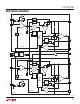
GSM Pulse Load
V
IN
RUN2 RUN1
LTC3619B
V
FB2
SW2
SW1
PGOOD1PGOOD2
V
FB1
22pF
RLIM GND
V
IN
3.4V TO 5.5V
V
OUT2
3.4V AT
800mA
V
OUT1
1.8V AT
400mA
3619B TA01
1190k
511k
255k
255k
1.5µH 3.3µH
2.2mF
×2
SuperCap
10µF
10µF
+
1000pF
116k
I
LIM
= 475mA
L, LT , LT C , LT M , Linear Technology, the Linear logo and Burst Mode are registered trademarks
and Hot Swap is a trademark of Linear Technology Corporation. All other trademarks are the
property of their respective owners. Protected by U.S. Patents, including 5481178, 6127815,
6304066, 6498466, 6580258, 6611131.
1ms/DIV
V
IN
= 5V, 500mA COMPLIANT
I
LOAD
= 0A to 2.2A, CHANNEL 1 UNLOADED
3619B TA01b
V
OUT
200mV/DIV
I
OUT
500mA/DIV
I
IN
500mA/DIV
V
IN
AC-COUPLED
1V/DIV