
Datasheet


LTC3619B
14
3619bfb
applicaTions inForMaTion
4. Other “hidden” losses, such as copper trace and internal
battery resistances, can account for additional efficiency
degradations in portable systems. It is very important
to include these “system” level losses in the design of a
system. The internal battery and fuse resistance losses
can be minimized by making sure that C
IN
has adequate
charge storage and very low ESR at the switching fre-
quency. Other losses, including diode conduction losses
during dead-time, and inductor core losses, generally
account for less than 2% total additional loss.
Thermal Considerations
In a majority of applications, the LTC3619B does not dis-
sipate much heat due to its high efficiency. In the unlikely
event that the junction temperature somehow reaches ap-
proximately 150°C, both power switches will be turned off
and the SW node will become high impedance. The goal
of the following thermal analysis is to determine whether
the power dissipated causes enough temperature rise to
exceed the maximum junction temperature (125°C) of the
part. The temperature rise is given by:
T
RISE
= P
D
• θ
JA
where P
D
is the power dissipated by the regulator and θ
JA
is the thermal resistance from the junction of the die to
the ambient
temperature.
The junction temperature, T
J
,
is given by:
T
J
= T
RISE
+ T
AMBIENT
As a worst-case example, consider the case when the
LTC3619B is in dropout on both channels at an input
voltage of 2.7V with a load current of 400mA and 800mA
and an ambient temperature of 70°C. From the Typical
Performance Characteristics graph of Switch Resistance,
the R
DS(ON)
of the switch is 0.56Ω and 0.33Ω. Therefore,
power dissipated by each channel is:
P
D1
= I
OUT
2
• R
DS(ON)
= 90mV
P
D2
= I
OUT
2
• R
DS(ON)
= 212mV
Given that the thermal resistance of a properly soldered
DFN package is approximately 40°C/W, the junction
temperature of an LTC3619B device operating in a 70°C
ambient temperature is approximately:
T
J
= (0.302W • 40°C/W) + 70°C = 82.1°C
which is well below the absolute maximum junction tem-
perature of 125°C.
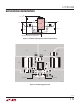
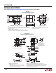
PC Board Layout Considerations
When laying out the printed circuit board, the following
checklist should be used to ensure proper operation of
the LTC3619B. These items are also illustrated graphically
in the layout diagrams of Figures 3a and 3b. Check the
following in your layout:
1. Does the capacitor C
IN
connect to the power V
IN
(Pin 6)
and GND (Pin 11) as closely as possible? This capacitor
provides the AC current of the internal power MOSFETs
and their drivers.
2. Are the respective C
OUT
and L closely connected? The
(–) plate of C
OUT
returns current to GND and the (–)
plate of C
IN
.
3. The resistor divider, R1 and R2, must be connected
between the (+) plate of C
OUT1
and a ground sense
line terminated near GND (Pin 11). The feedback sig-
nals V
FB1
and V
FB2
should be routed away from noisy
components and traces, such as the SW lines (Pins 5
and 7), and their trace length should be minimized.
4. Keep sensitive components away from the SW pins, if
possible. The input capacitor C
IN
, C
LIM
and the resistors
R1, R2, R3 and R4 and R
LIM
should be routed away
from the SW traces and the inductors.
5. A ground plane is preferred, but if not available, keep
the signal and power grounds segregated with small
signal components returning to the GND pin at a single
point. These ground traces should not share the high
current path of C
IN
or C
OUT
.
6. Flood all unused areas on all layers with copper.
Flooding with copper will reduce
the temperature
rise
of power components. These copper areas should be
connected to V
IN
or GND.