
Datasheet


LTC3633A-2/LTC3633A-3
15
3633a23f
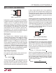
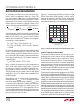
Figure 3. Setting the Output Voltage
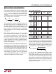
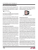
Figure 2. Diode-OR Circuit
FB
R2
R1
C
F
3633a23 F02
V
OUT
SGND
LTC3633A-2
APPLICATIONS INFORMATION
Furthermore, as long as SV
IN
is powered, the LTC3633A-2/
LTC3633A-3 operates as a step-down regulator with PV
IN
voltages as low as 1.5V (subject to minimum off-time
constraints). However, at PV
IN
voltages less than 3V, in-
ternal on-time calculation errors increase, and controlled
on-time operation is not guaranteed. If this occurs, the
output voltages will remain in regulation, but the switch-
ing frequency of each channel may deviate from the
programmed frequency under these conditions and phase
lock between the two channels may be lost.
Boost Capacitor
The LTC3633A-2 uses a “bootstrap” circuit to create a
voltage rail above the applied input voltage PV
IN
. Specifi -
cally, a boost capacitor, C
BOOST
, is charged to a voltage
approximately equal to INTV
CC
each time the bottom power
MOSFET is turned on. The charge on this capacitor is then
used to supply the required transient current during the
remainder of the switching cycle. When the top MOSFET
is turned on, the BOOST pin voltage will be equal to ap-
proximately PV
IN
+ 3.3V. For most applications, a 0.1µF
ceramic capacitor closely connected between the BOOST
and SW pins will provide adequate performance.
Output Voltage Programming
Each regulator’s output voltage is set by an external resis-
tive divider according to the following equation:
V
OUT
= 0.6V 1+
R2
R1
⎛
⎝
⎜
⎞
⎠
⎟
The desired output voltage is set by appropriate selection
of resistors R1 and R2 as shown in Figure 3. Choosing
large values for R1 and R2 will result in improved zero-
load effi ciency but may lead to undesirable noise coupling
or phase margin reduction due to stray capacitances
at the V
FB
node. Care should be taken to route the V
FB
trace away from any noise source, such as the SW trace.
To improve the frequency response of the main control
loop, a feedforward capacitor, C
F
, may be used as shown
in Figure 3.
Connecting the V
ON
pin to the output voltage makes the
on-time proportional the output voltage and allows the
internal on-time servo loop to lock the converter’s switching
frequency to the programmed value. If the output voltage
is outside the V
ON
sense range (0.6V – 6V for LTC3633A-2,
1.5V – 12V for LTC3633A-3), the output voltage will stay
in regulation, but the switching frequency may deviate
from the programmed frequency.
Minimum Off-Time/On-Time Considerations
The minimum off-time is the smallest amount of time that
the LTC3633A-2 can turn on the bottom power MOSFET,
trip the current comparator and turn the power MOSFET
back off. This time is typically 45ns. For the controlled
on-time architecture, the minimum off-time limit imposes
a maximum duty cycle of:
DC
(MAX)
= 1–f • t
OFF(MIN)
+ 2•t
DEAD
()
where f is the switching frequency, t
DEAD
is the nonoverlap
time, or “dead time” (typically 10ns) and t
OFF(MIN)
is the
minimum off-time. If the maximum duty cycle is surpassed,
due to a dropping input voltage for example, the output
will drop out of regulation. The minimum input voltage to
avoid this dropout condition is:
V
IN(MIN)
=
V
OUT
1− f• t
OFF(MIN)
+ 2•t
DEAD
()
SUPPLY1
PV
IN1
PV
IN2
SV
IN
3633a23 F02
SUPPLY2
LTC3633A-2