
Datasheet


LTC3633A/LTC3633A-1
15
3633a1f
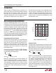
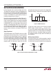
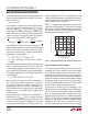
Figure 2. Setting the Output Voltage
FB
R2
R1
C
F
3633a F02
V
OUT
SGND
LTC3633A
APPLICATIONS INFORMATION
Low Power 2.5V Linear Regulator
The V2P5 pin can be used as a low power 2.5V regulated
rail. This pin is the output of a 10mA linear regulator
powered from the INTV
CC
pin. Note that the power from
V2P5 eventually comes from V
IN1
since the INTV
CC
power
is supplied from V
IN1
. When using this output, this pin
must be bypassed with a 1µF ceramic capacitor. If this
output is not being used, it is recommended to short this
output to INTV
CC
to disable the regulator.
Output Voltage Programming
Each regulator’s output voltage is set by an external resis-
tive divider according to the following equation:
V
OUT
= 0.6V 1+
R2
R1
⎛
⎝
⎜
⎞
⎠
⎟
The desired output voltage is set by appropriate selection
of resistors R1 and R2 as shown in Figure 2. Choosing
large values for R1 and R2 will result in improved zero-
load effi ciency but may lead to undesirable noise coupling
or phase margin reduction due to stray capacitances
at the V
FB
node. Care should be taken to route the V
FB
trace away from any noise source, such as the SW trace.
To improve the frequency response of the main control
loop, a feedforward capacitor, C
F
, may be used as shown
in Figure 2.
Connecting the V
ON
pin to the output voltage makes the
on-time proportional the output voltage and allows the
internal on-time servo loop to lock the converter’s switching
frequency to the programmed value. If the output voltage
is outside the V
ON
sense range (0.6V – 6V for LTC3633A,
1.5V – 12V for LTC3633A-1), the output voltage will stay
in regulation, but the switching frequency may deviate
from the programmed frequency.
Minimum Off-Time/On-Time Considerations
The minimum off-time is the smallest amount of time that
the LTC3633A can turn on the bottom power MOSFET,
trip the current comparator and turn the power MOSFET
back off. This time is typically 45ns. For the controlled
on-time architecture, the minimum off-time limit imposes
a maximum duty cycle of:
DC
(MAX)
= 1– f• t
OFF(MIN)
+ 2•t
DEAD
()
where f is the switching frequency, t
DEAD
is the nonoverlap
time, or “dead time” (typically 10ns), and t
OFF(MIN)
is the
minimum off-time. If the maximum duty cycle is surpassed,
due to a dropping input voltage for example, the output
will drop out of regulation. The minimum input voltage to
avoid this dropout condition is:
V
IN(MIN)
=
V
OUT
1− f• t
OFF(MIN)
+ 2•t
DEAD
()
Conversely, the minimum on-time is the smallest dura-
tion of time in which the top power MOSFET can be in
its “on” state. This time is typically 20ns. In continuous
mode operation, the minimum on-time limit imposes a
minimum duty cycle of:
DC
(MIN)
= f•t
ON(MIN)
()
where t
ON(MIN)
is the minimum on-time. As the equation
shows, reducing the operating frequency will alleviate the
minimum duty cycle constraint.
In the rare cases where the minimum duty cycle is
surpassed, the output voltage will still remain in regula-
tion, but the switching frequency will decrease from its
programmed value. This constraint may not be of critical
importance in most cases, so high switching frequencies
may be used in the design without any fear of severe
consequences. As the sections on Inductor and Capacitor
selection show, high switching frequencies allow the use
of smaller board components, thus reducing the footprint
of the application circuit.