
Datasheet


LTC3721-1
12
sn37211 37211fs
OPERATIO
U
Leading Edge Blanking
The LTC3721-1 provides programmable leading edge
blanking to prevent nuisance tripping of the current sense
circuitry. Leading edge blanking relieves the filtering re-
quirements for the CS pin, greatly improving the response
to real overcurrent conditions. It also allows the use of a
ground referenced current sense resistor or transformer(s),
further simplifying the design. With a single 10k to 100k
resistor from R
LEB
to GND, blanking times of approxi-
mately 40ns to 320ns are programmed. If not required,
connecting R
LEB
to V
REF
can disable leading edge blank-
ing. Keep in mind that the use of leading edge blanking will
slightly reduce the linear control range for the pulse width
modulator.
High Current Drivers
The LTC3721-1 high current, high speed drivers provide
direct drive of external power N-channel MOSFET switches.
The drivers swing from rail to rail. Due to the high pulsed
current nature of these drivers (1.5A sink, 1A source), care
must be taken with the board layout to obtain advertised
performance. Bypass V
CC
with a 1µF minimum, low ESR,
ESL ceramic capacitor. Connect this capacitor with mini-
mal length PCB leads to both V
CC
and GND. A ground plane
is highly recommended. The driver output pins (DRVA,
DRVB) connect to the gates of the external MOSFET
switches. The PCB traces making these connections should
also be as short as possible to minimize overshoot and
undershoot of the drive signal.
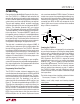
Transformer Configurations
The LTC3721-1 used in a typical isolated push-pull con-
verter application will need a transformer to provide the
voltage translation and galvanic isolation. The push-pull
transformer employs a center tapped primary winding
configuration. The transformer secondary can be center
tapped or a single winding depending on the configuration
and application needs.
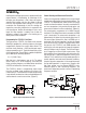
Center tapped secondary configurations apply alternating
<50% duty cycle square waves to a single inductor/
capacitor combination. This L-C circuit filters the square
wave and produces the regulated output voltage. The
secondary square wave amplitude is given by:
V
SEC
= V
IN
• N, where N = Ns/Np, transformer turns
ratio, # of secondary turns divided by # of primary
turns.