
Datasheet


LTC3721-1
7
sn37211 37211fs
FB (Pin 13/Pin 12): Error Amplifier Inverting Input. This is
the voltage feedback input for the LTC3721-1. The nomi-
nal regulation voltage at FB is 1.2V.
SS (Pin 14/Pin 13): Soft-Start/Restart Delay Circuitry
Timing Capacitor. A capacitor from SS to GND provides a
controlled ramp of the current command. During overload
conditions, SS is discharged to ground initiating a soft-
start cycle. SS charging current is approximately 13µA. SS
will charge up to approximately 5V in normal operation.
During a constant overload current fault, SS will oscillate
at a low frequency between approximately 0.5V and 4V.
DESCRIPTIO S
U
PI
U
UVLO (Pin 15/Pin 14): Input to Program System Turn-On
and Turn-Off Voltages. The nominal threshold of the UVLO
comparator is 5.0V. UVLO is connected to the main DC
system feed through a resistor divider. When the UVLO
threshold is exceeded, the LTC3721-1 commences a soft-
start cycle and a 10µA (nominal) current is fed out of UVLO
to program the desired amount of system hysteresis. The
hysteresis level can be adjusted by changing the resis-
tance of the divider. UVLO can also be used to terminate
all switching by pulling UVLO down to less than 4V. An
open drain or collector switch can perform this function
without changing the system turn on or turn off voltages.
NC (Pin 2, Pin 3, Pin 16/Pin 7, Pin 16): Not Connected.
(GN Package/UF Package)
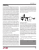
PROGRAMMABLE
DEAD-TIME
DRVA
DRVB
37211 TD01
CURRENT
SENSE
OR C
T
RAMP
PWM
COMPARATOR
(–)
TI I G DIAGRA
WUW