
Datasheet


LTC3728L/LTC3728LX
25
3728lxff
applicaTions inForMaTion
If V
SEC
drops below this level, the FCB voltage forces
temporary continuous switching operation until V
SEC
is
again above its minimum.
In order to prevent erratic operation if no external connec-
tions are made to the FCB pin, the FCB pin has a 0.18µA
internal current source pulling the pin high. Include this
current when choosing resistor values R5 and R6.
The following table summarizes the possible states avail-
able on the FCB pin:
Table 1
FCB Pin Condition
0V to 0.75V Forced Continuous Both Controllers
(Current Reversal Allowed— Burst Inhibited)
0.85V < V
FCB
< 4.3V Minimum Peak Current Induces
Burst Mode Operation
No Current Reversal Allowed
Feedback Resistors Regulating a Secondary Winding
>4.8V Burst Mode Operation Disabled
Constant-Frequency Mode Enabled
No Current Reversal Allowed
No Minimum Peak Current
Voltage Positioning
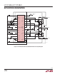
Voltage positioning can be used to minimize peak-to-peak
output voltage excursions under worst-case transient
loading conditions. The open-loop DC gain of the control
loop is reduced depending upon the maximum load step
specifications. Voltage positioning can easily be added
to either or both controllers by loading the I
TH
pin with
a resistive divider having a Thevenin equivalent voltage
source equal to the midpoint operating voltage range of
the error amplifier, or 1.2V (see Figure 8).
The resistive load reduces the DC loop gain while main-
taining the linear control range of the error amplifier. The
maximum output voltage deviation can theoretically be
reduced to half, or alternatively the amount of output
capacitance can be reduced for a particular application.
A complete explanation is included in Design Solutions
10 (see www.linear.com).
Efficiency Considerations
The percent efficiency of a switching regulator is equal to
the output power divided by the input power times 100%.
It is often useful to analyze individual losses to determine
what is limiting the efficiency and which change would
produce the most improvement. Percent efficiency can
be expressed as:
%Efficiency = 100% – (L1 + L2 + L3 + ...)
where L1, L2, etc. are the individual losses as a percent-
age of input power.
Although all dissipative elements in the circuit produce
losses, four main sources usually account for most of the
losses in LTC3728L/LTC3728LX circuits: 1) IC V
IN
current
(including loading on the 3.3V internal regulator), 2) IN-
TV
CC
regulator current, 3) I
2
R losses, 4) Topside MOSFET
transition losses.
1. The V
IN
current has two components: the first is the
DC supply current given in the Electrical Characteristics
table, which excludes MOSFET driver and control cur-
rents; the second is the current drawn from the 3.3V
linear regulator output. V
IN
current typically results in
a small (<0.1%) loss.
2. INTV
CC
current is the sum of the MOSFET driver and
control currents. The MOSFET driver current results from
switching the gate capacitance of the power MOSFETs.
Each time a MOSFET gate is switched from low to high
to low again, a packet of charge dQ moves from INTV
CC
to ground. The resulting dQ/dt is a current out of INTV
CC
that is typically much larger than the control circuit
current. In continuous mode, I
GATECHG
= f(Q
T
+ Q
B
),
where Q
T
and Q
B
are the gate charges of the topside
and bottom side MOSFETs.
Figure 8. Active Voltage Positioning
Applied to the LTC3728L/LTC3728LX
I
TH
R
C
R
T1
INTV
CC
C
C
3728 F08
LTC3728L/
LTC3728LX
R
T2