
Datasheet


LTC3728L/LTC3728LX
27
3728lxff
applicaTions inForMaTion
produce output voltage and I
TH
pin waveforms that will
give a sense of the overall loop stability without break-
ing the feedback loop. Placing a power MOSFET directly
across the output capacitor and driving the gate with an
appropriate signal generator is a practical way to produce
a realistic load step condition. The initial output voltage
step resulting from the step change in output current may
not be within the bandwidth of the feedback loop, so this
signal cannot be used to determine phase margin. This
is why it is better to look at the I
TH
pin signal, which is
in the feedback loop and is the filtered and compensated
control loop response. The gain of the loop will be in-
creased by increasing R
C
and the bandwidth of the loop
will be increased by decreasing C
C
. If R
C
is increased by
the same factor that C
C
is decreased, the zero frequency
will be kept the same, thereby keeping the phase shift the
same in the most critical frequency range of the feedback
loop. The output voltage settling behavior is related to the
stability of the closed-loop system and will demonstrate
the actual overall supply performance.
A second, more severe transient is caused by switching
in loads with large (>1µF) supply bypass capacitors. The
discharged bypass capacitors are effectively put in parallel
with C
OUT
, causing a rapid drop in V
OUT
. No regulator can
alter its delivery of current quickly enough to prevent this
sudden step change in output voltage if the load switch
resistance is low and it is driven quickly. If the ratio of
C
LOAD
to C
OUT
is greater than 1:50, the switch rise time
should be controlled so that the load rise time is limited
to approximately 25 • C
LOAD
. Thus a 10µF capacitor would
require a 250µs rise time, limiting the charging current
to about 200mA.
Automotive Considerations: Plugging into the
Cigarette Lighter
As battery-powered devices go mobile, there is a natural
interest in plugging into the cigarette lighter in order to
conserve or even recharge battery packs during operation.
But before you connect, be advised: you are plugging
into the supply from hell. The main power line in an
automobile is the source of a number of nasty potential
transients, including load-dump, reverse-battery and
double-battery.
Load-dump is the result of a loose battery cable. When the
cable breaks connection, the field collapse in the alterna-
tor can cause a positive spike as high as 60V which takes
several hundred milliseconds to decay. Reverse-battery is
just what it says, while double-battery is a consequence of
tow truck operators finding that a 24V jump start cranks
cold engines faster than 12V.
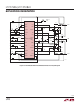
The network shown in Figure 9 is the most straightforward
approach to protect a DC/DC converter from the ravages of
an automotive power line. The series diode prevents current
from flowing during reverse-battery, while the transient
suppressor clamps the input voltage during load-dump.
Note that the transient suppressor should not conduct
during double-battery operation, but must still clamp the
input voltage below breakdown of the converter. Although
the LTC3728L/LTC3728LX have a maximum input voltage
of 30V, most applications will also be limited to 30V by
the MOSFET BVD
SS
.
Figure 9. Automotive Application Protection
V
IN
3728 F09
LTC3728L/
LTC3728LX
TRANSIENT VOLTAGE
SUPPRESSOR
GENERAL INSTRUMENT
1.5KA24A
50A I
PK
RATING
12V